
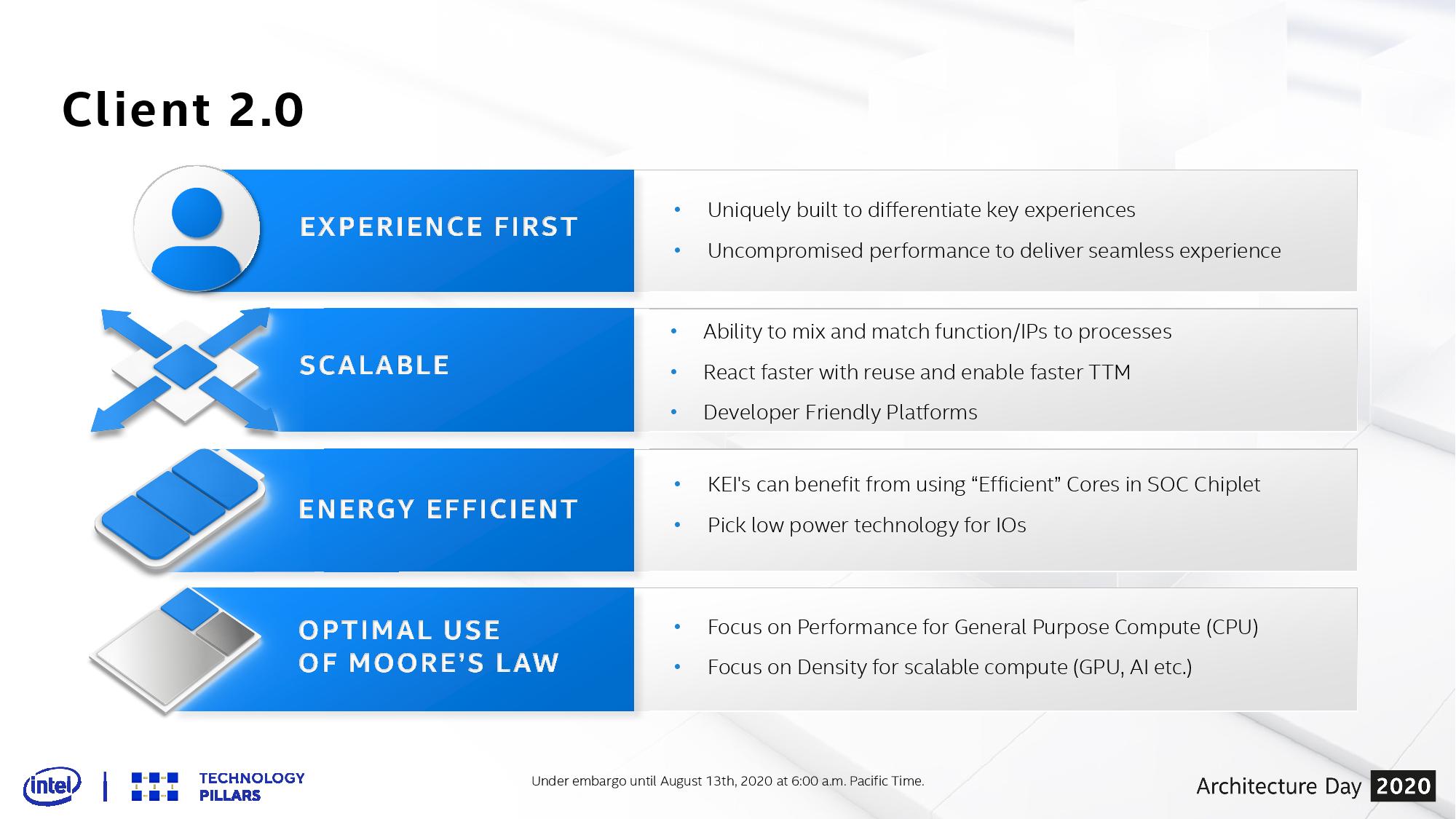
One of the extra esoteric components of Intel’s Architecture Day 2020 got here very close to the top, the place Intel spent a couple of minutes discussing what it believes is the way forward for a few of its merchandise. Brijesh Tripathi, VP and CTO of Intel’s Client Computing group, laid out a imaginative and prescient about the way forward for its consumer merchandise within the 2024+ future timeframe. Centered round Intel’s 7+ manufacturing course of, the aim was to allow ‘Client 2.0’ – a brand new approach to ship and allow immersive experiences by means of a extra optimized silicon improvement technique.
Chiplets aren’t new, particularly with latest launches from Intel’s opponents, and as we transfer into extra advanced course of node improvement, the period of chiplets permits sooner time-to-market in addition to higher binning and yields for a given product. The secret’s enabling how these chiplets match collectively, and at which factors it is smart to combine and match the related ones. Intel has spoken about this earlier than in a extra generalized context, at its Technology and Manufacturing Day 2017, as proven within the carousel picture on the high.
The aim right here is to combine and match which course of nodes work greatest for various elements of the chip. Intel appears set to comprehend this imaginative and prescient beginning with its 7nm platform. At Architecture Day 2020, Brijesh Tripathi confirmed this slide:
On the left is a typical chip design – monolithic with every thing it requires. For Intel’s forefront merchandise, these take 3-Four years to develop, and bugs are present in silicon by each Intel initially after which later by Intel’s companions as they will ramp up the silicon-on time by a a number of orders of magnitude.
In the center is a fundamental chiplet structure, just like that slide from 2017, the place completely different capabilities of the die are cut up into their very own modules. Assuming a constant interconnect, there are some reuse of the silicon components, reminiscent of AMD utilizing the identical core compute dies in consumer and server. For some semiconductor corporations (besides Intel), that is the place we’re.
On the suitable is the place Intel sees its future. Instead of getting a single digit variety of chiplets in a product, it envisions a world the place every IP might be cut up into a number of chiplets, enabling merchandise to be constructed with completely different configurations of what works for the market. In this occasion, a chiplet may be a PCIe 4.zero x16 hyperlink – if the product wants extra, it merely provides in additional of those chiplets. Same with reminiscence channels, cores, media accelerators, AI accelerators, Ray Tracing engines, crypto accelerators, graphics, and even as far down as SRAM and caching blocks. The thought is that every IP might be cut up after which scaled. This implies that the chiplets are tiny, might be constructed comparatively shortly, and bugs must be ironed out in a short time.

In this diagram, we’re handled to Intel’s long run imaginative and prescient for the consumer – a base interposer with an in-package reminiscence (one thing like an L3 or L4) that may act as the primary SRAM cache for the entire die, after which on high of this we get 24 completely different chiplets. Chiplets might be graphics, cores, AI, Media, IO, or anything, however they are often blended and matched based mostly on what is required. A content material creator would possibly need a stability between some good graphics acceleration and compute, whereas a gamer would possibly wish to focus purely on the graphics. A company consumer or workstation would possibly want much less graphics and extra for compute and AI, whereas a cellular model of the chip can be closely invested in IO.
As all the time, there’s some trade-off between chiplet measurement and complexity of truly placing them collectively in a multi-die association. Any communications between chiplets prices extra energy than a monolithic interpretation, and often supply greater latency. Thermals must be managed as properly, and so generally these chiplets are restricted by…


