
TSMC has been providing its System-on-Wafer integration know-how, InFO-SoW, since 2020. For now, solely Cerebras and Tesla have developed wafer scale processor designs utilizing it, as whereas they’ve incredible efficiency and energy effectivity, wafer-scale processors are extraordinarily advanced to develop and produce. But TSMC believes that not solely will wafer-scale designs ramp up in utilization, however that megatrends like AI and HPC will name for much more advanced options: vertically stacked system-on-wafer designs.
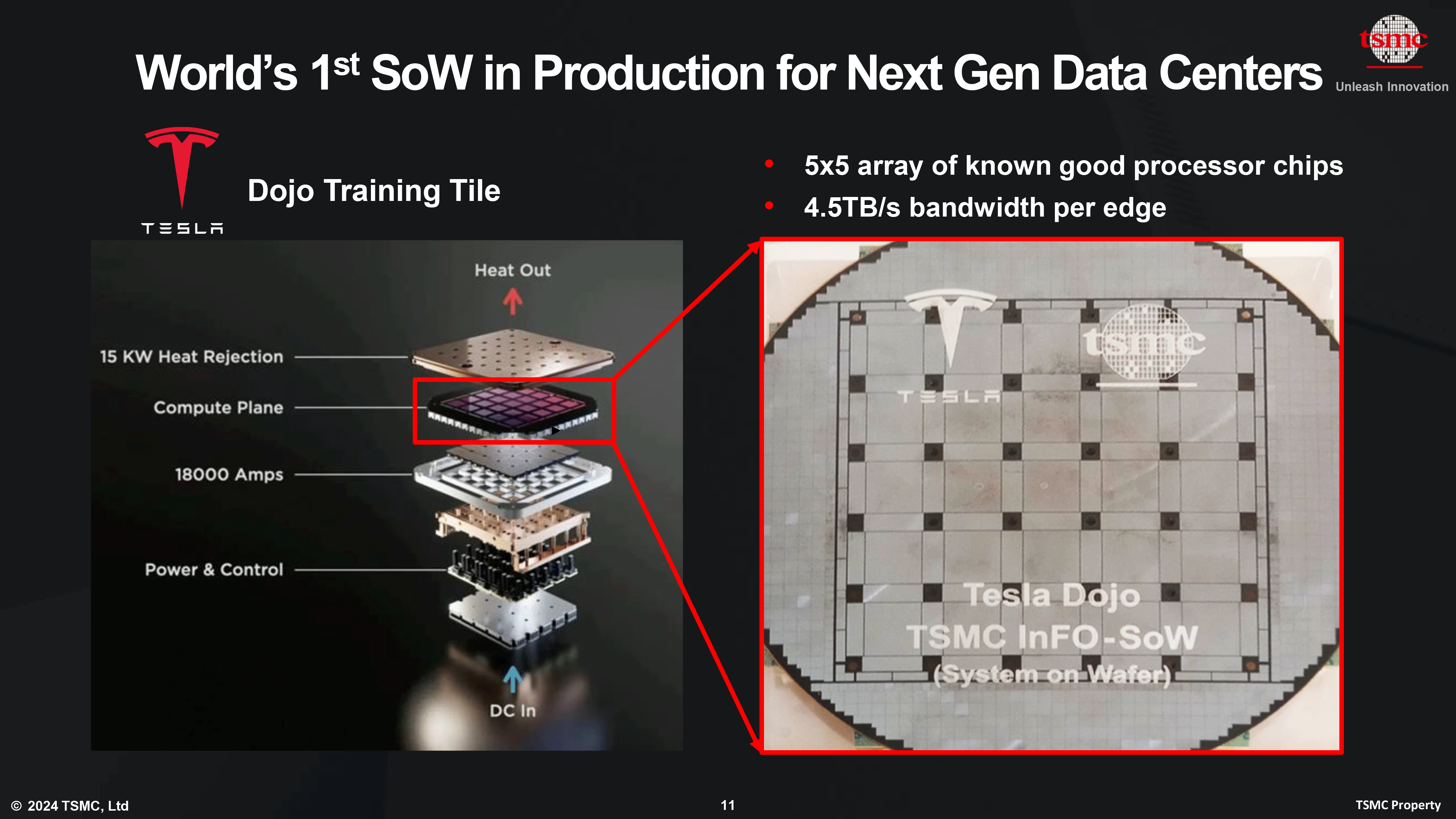
Tesla Dojo’s wafer-scale processors — the primary options based mostly based mostly on TSMC’s InFO-SoW know-how which can be in mass manufacturing — have a number of advantages over typical system-in-packages (SiPs), together with low-latency high-bandwidth core-to-core communications, very excessive efficiency and bandwidth density, comparatively low energy supply community impendance, excessive efficiency effectivity, and redunancy.
But with InFO-SoW and different wafer scale integration strategies, processor designers need to rely solely on on-chip reminiscence. This is completely ample for a lot of purposes, however it might not be sufficient for next-generation AI workloads. Furthermore, with InFO-SoW, the entire wafer needs to be processed utilizing one fabrication know-how, which might not be optimum, or too costly for sure designs.
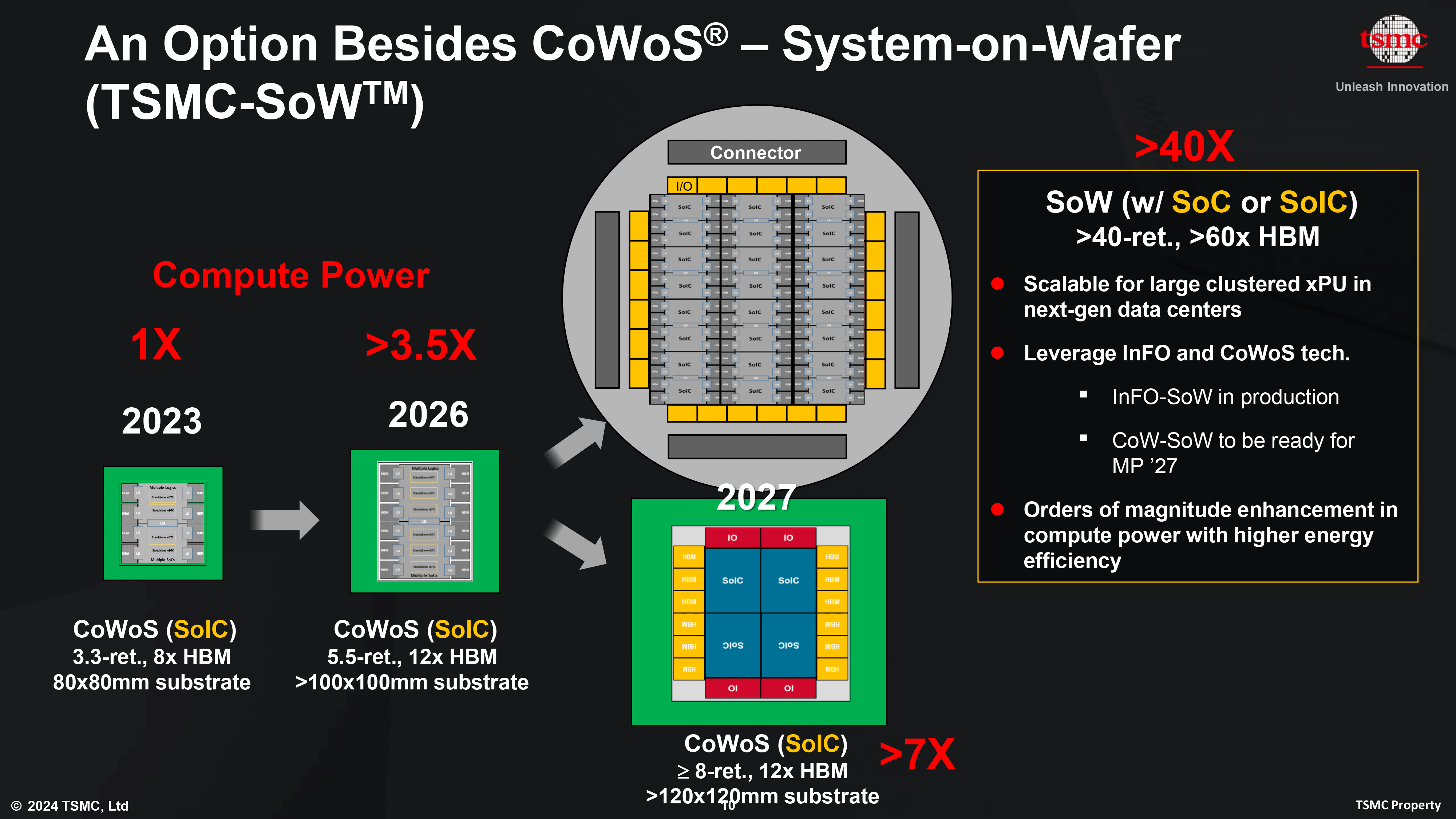
So, with its next-generation system-on-wafer platform, TSMC plans to convey collectively two of its packaging applied sciences: InFO-SoW and System on Integrated Chips (SoIC), which can permit it to stack reminiscence or logic on prime of a system-on-wafer utilizing its Chip-on-Wafer (CoW) methodology. The CoW-SoW know-how, which the corporate introduced at its North American Technology Symposium, shall be prepared for mass manufacturing in 2027.
For now, TSMC is usually speaking about marriage ceremony wafer scale processors with HBM4 reminiscence. And on condition that HBM4 stacks will function a 2048-bit interface, its tighter integration with logic is one thing that the business is contemplating.
“So, in the future, using wafer level integrations [will allow] our customers to integrate even more logic and memory together,” stated Kevin Zhang, Vice President of Business Development at TSMC. “SoW is no longer a fiction, this is something we already work with our customers [on] to produce some of the products already in place. This we think by leveraging our advanced wafer level integration technology, we can provide our customer a very important the path allow them to continue to grow their capability to bring in more computation, more energy efficient computation, to their AI cluster or [supercomputer].”


