
With the arrival of spring comes showers, flowers, and within the expertise trade, TSMC’s annual expertise symposium collection. With clients unfold all world wide, the Taiwanese pure play foundry has adopted an fascinating technique for updating its clients on its fab plans, holding a collection of symposiums from Silicon Valley to Shanghai. Kicking off the collection yearly – and giving us our first actual take a look at TSMC’s up to date foundry plans for the approaching years – is the Santa Clara cease, the place yesterday the corporate has detailed a number of new applied sciences, starting from extra superior lithography processes to huge, wafer-scale chip packing choices.
Today we’re publishing a number of tales primarily based on TSMC’s completely different choices, beginning with TSMC’s marquee announcement: their A16 course of node. Meanwhile, for the remainder of our symposium tales, please you’ll want to take a look at the associated studying under, and examine again for extra tales.
Headlining its Silicon Valley cease, TSMC introduced its first ‘angstrom-class’ course of expertise: A16. Following a manufacturing schedule shift that has seen bottom energy supply community expertise (BSPDN) faraway from TSMC’s N2P node, the brand new 1.6nm-class manufacturing node will now be the primary course of to introduce BSPDN to TSMC’s chipmaking repertoire. With the addition of bottom energy capabilities and different enhancements, TSMC expects A16 to supply considerably improved efficiency and vitality effectivity in comparison with TSMC’s N2P fabrication course of. It will likely be accessible to TSMC’s shoppers beginning H2 2026.
TSMC A16: Combining GAAFET With Backside Power Delivery
At a excessive degree, TSMC’s A16 course of expertise will depend on gate-all-around (GAAFET) nanosheet transistors and can characteristic a bottom energy rail, which is able to each enhance energy supply and reasonably enhance transistor density. Compared to TSMC’s N2P fabrication course of, A16 is anticipated to supply a efficiency enchancment of 8% to 10% on the similar voltage and complexity, or a 15% to 20% discount in energy consumption on the similar frequency and transistor depend. TSMC just isn’t itemizing detailed density parameters this far out, however the firm says that chip density will enhance by 1.07x to 1.10x – preserving in thoughts that transistor density closely relies on the kind and libraries of transistors used.
The key innovation of TSMC’s A16 node, is its Super Power Rail (SPR) bottom energy supply community, a primary for TSMC. The contract chipmaker claims that A16’s SPR is particularly tailor-made for high-performance computing merchandise that characteristic each complicated sign routes and dense energy circuitry.
As famous earlier, with this week’s announcement, A16 has now change into the launch car for bottom energy supply at TSMC. The firm was initially slated to supply BSPDN expertise with N2P in 2026, however for causes that are not fully clear, the tech has been punted from N2P and moved to A16. TSMC’s official timing for N2P in 2023 was at all times a bit unfastened, so it is laborious to say if this represents a lot of a sensible delay for BSPDN at TSMC. But on the similar time, it is essential to underscore that A16 is not simply N2P renamed, however quite it is going to be a definite expertise from N2P.
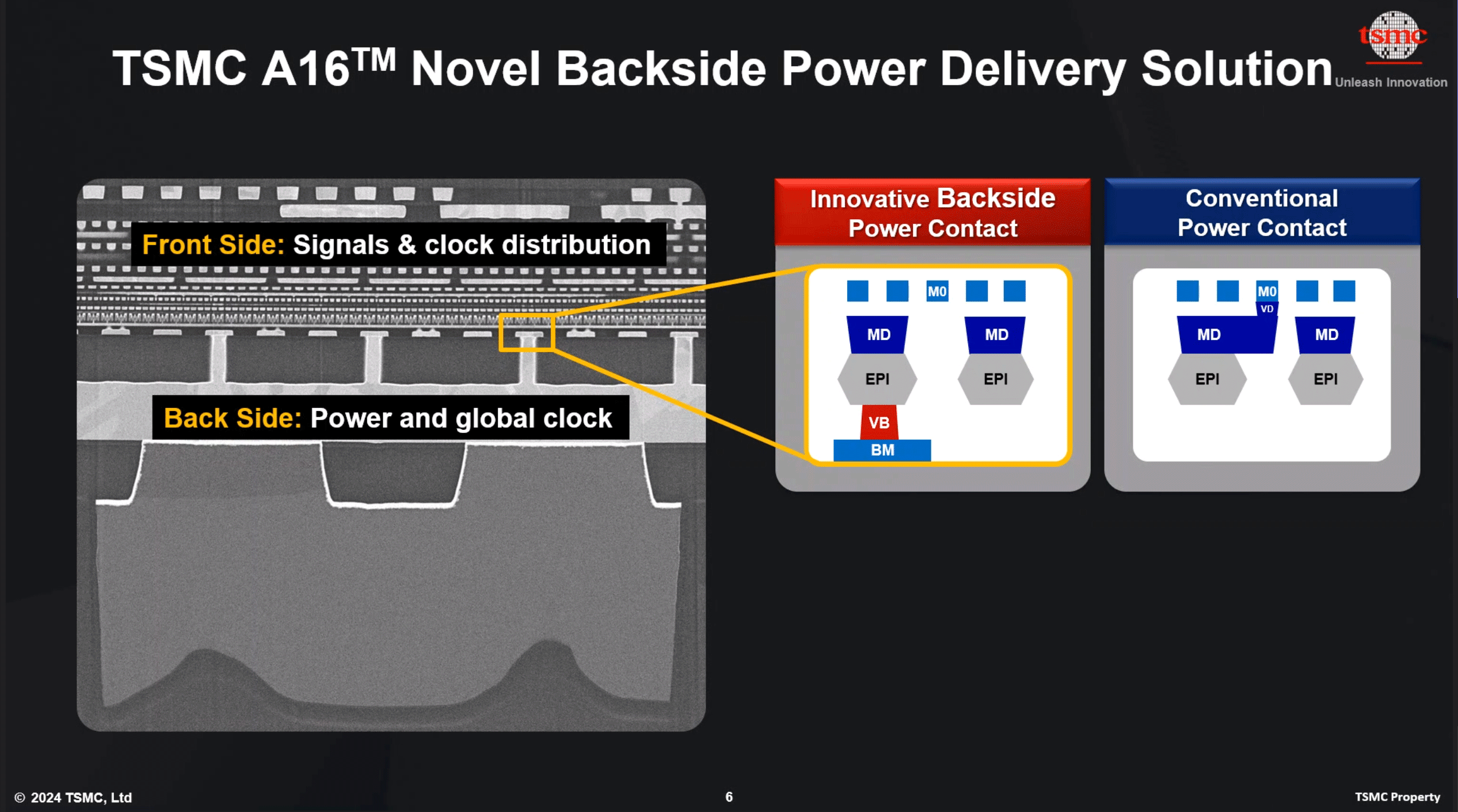
TSMC just isn’t the one fab pursuing bottom energy supply, and accordingly, we’re seeing a number of variations on the approach crop up at completely different fabs. The total trade has three approaches for BSPDN: Imec’s Buried Power Rail, Intel’s PowerBy way of, and now TSMC’s Super Power Rail.
The oldest approach, Imec’s Buried Power Rail, primarily locations energy supply community on the bottom of the wafer after which connects energy rail of logic cells to energy contact utilizing nano TSVs. This allows some space scaling and doesn’t add an excessive amount of complexity to manufacturing. The…

