
HBM2E boasts high-speed, high-capacity, and low-power traits; it’s an optimum reminiscence answer for the next-generation AI (Artificial Intelligence) programs together with Deep Learning Accelerator and High-Performance Computing, which all require high-level computing efficiency. Furthermore, it’s anticipated to be utilized to the Exascale supercomputer – a high-performance computing system which might carry out calculations a quintillion instances per second – that may lead the analysis of next-generation fundamental and utilized science, similar to local weather modifications, bio-medics, and area exploration.
“SK hynix has been in the forefront of technology innovation that contributes to human civilization with achievements including the world’s first development of HBM products,” stated Jonghoon Oh, Executive Vice President and Chief Marketing Officer (CMO) at SK hynix. “With the full-scale mass-production of HBM2E, we will continue to strengthen our presence in the premium memory market and lead the fourth industrial revolution.”
Annotation
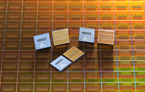
■ HBM (High Bandwidth Memory)
- High efficiency, excessive bandwidth reminiscence merchandise that undertake TSV know-how to dramatically speed up information processing pace over conventional DRAMs.
■ TSV (Through Silicon Via)
- An interconnecting know-how that connects the higher and decrease chips by means of 1000’s of high quality holes on DRAM chip.
- Delivers information, instructions, and currents by means of column-shaped paths that penetrate all the silicon wafer thickness after stacking a number of DRAM chips on the buffer chip.
- Up to 30% lower in dimension and as much as 50% lower in energy consumption over current packaging strategies.
■ Standards for information course of pace conversion
- 1 GB = 8Gb
- 3.6 Gbps per pin with 1024 information I/Os (Inputs/Outputs) = 3686.4 Gbps
- 3686.4 Gbps / 8 = 460.Eight GB/s (Gb -> GB conversion)


