SK Hynix this week announced financial results for its fiscal year 2016 and also revealed general plans for 2017. As expected, the company intends to start volume production of new types of memory and expand production capacities. What is noteworthy is that the company will primarily invest in the expansion of NAND flash manufacturing capacities, rather than the expansion of DRAM production, in the short-term future.
DRAM: 21 nm Ramping, 18 nm(?) on Track for 2H 2017
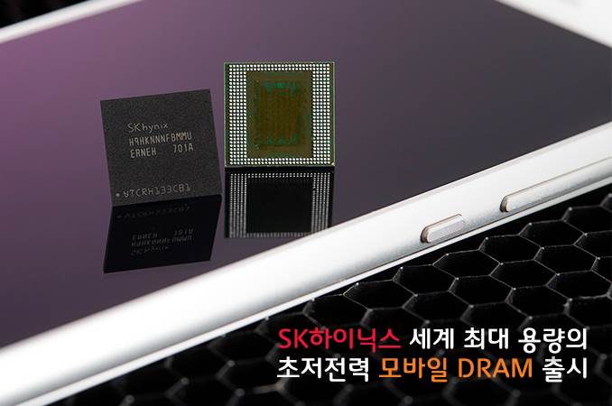
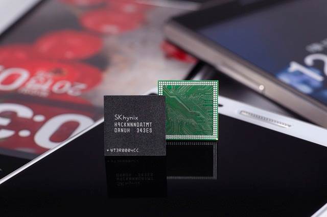
SK Hynix began to make DRAM using its 21 nm fabrication process in late 2015. The manufacturer has been gradually expanding usage of the technology as well as improving its yields since then. By now, SK Hynix makes a wide range of its products (including mainstream DRAM, mobile DRAM and specialized memory) using its 21 nm manufacturing process. This week the company confirmed that it intends to start volume production of DRAM using its 10 nm-class process technology (which industry experts believe is 18 nm) this year.

Just like other memory makers, SK Hynix plans to be conservative about its DRAM capital expenditures in 2017 and at present the company does not plan to undertake any significant capacity expansions. In the meantime, further increase of DRAM production using the 21 nm fabrication process and the start of 18 nm DRAM volume ramp in the second half of 2017 will automatically boost SK Hynix’s DRAM bit output — as memory cells get smaller, it is possible to produce more bits using one 300 mm wafer.
Meanwhile, analysts from TrendForce believe that DRAM bit demand in 2017 will surpass 20% year-over-year, whereas DRAM bit supply by various makers will increase by around 19% YoY. The imbalance between demand and supply is projected to create shortages of DRAM as well as keep prices at high levels. Apart from PCs, there are two more factors that are going to raise demand for memory: first, Intel’s upcoming Xeon platform ‘Purley’ is expected to drive demand; and second, higher-end Google Android-based smartphones are expected to receive a memory upgrade with top-of-the-range models holding 8 GB of LPDDR4/LPDDR4X.
NAND: 72-Layer 512 Gb Chips Due in Late 2017
Demand for NAND flash has been steadily increasing in the recent years because the industry is increasing output of NAND-based devices (e.g., smartphones, SSDs, consumer electronics, etc.) as well as its content per box (e.g., the entry-level Apple iPhone 7 now contains 32 GB of storage, up from 16 GB). To meet the growing demand, manufacturers expand production capacities and introduce higher-capacity 3D NAND memory chips. Just like its competitors, SK Hynix plans to boost production of NAND in general and launch new ICs.

SK Hynix started to mass-produce its 36-layer 128 Gb 3D MLC NAND (which it calls 3D-V2) chips in 2015 and these ICs have been primarily used for various removable storage products. Last year, the company also started to make 48-layer 3D NAND (3D-V3) ICs that are to be used for various types of memory cards, flash drives, embedded storage and SSDs. With its third-gen 3D NAND, SK Hynix focuses on 256 Gb (32 GB) TLC ICs. The latter are used to build various NAND packages with 256 Gb, 512 Gb, 1024 Gb, 2048 Gb and even 4096 Gb capacities, which can be used for a variety of applications.
Later this year SK Hynix intends to start volume production of 72-layer 3D TLC NAND (3D-V4) memory and this is where things start to get interesting. Initially, SK Hynix intends to produce 256 Gb 3D TLC ICs and these are going to be available already in Q2 2017, according to the company’s product catalog. Later on, sometimes in Q4, the company plans to introduce 512 Gb 3D TLC ICs (64 GB), which will help it to significantly increase capacities of SSDs and other devices featuring NAND flash. What is important about SK Hynix’s fourth-gen 3D NAND is that it will feature block size of 13.5 MB, which will increase the performance of such ICs compared to 3D-V3 and 3D-V2 that have a block size of 9 MB. At this point, we do not know whether SK Hynix intends to increase interface speed of its 512 Gb 3D-V4 ICs to compensate lower parallelism in lower-capacity SSDs, like Samsung did with its high-capacity 64-layer 3D V-NAND chips. What we do know is that SK Hynix’s catalog already includes NAND multi-chip packages of 8192 Gb capacity (1 TB) that will enable high-capacity SSDs in smaller form-factors (e.g., 2 GB single-sided M.2). Meanwhile, 64 GB NAND flash chips may force SK Hynix and its partners to abandon low-capacity SSDs (i.e., 120/128 GB) unless there is sufficient demand.
M14 Fab Gets Second Layer Floor
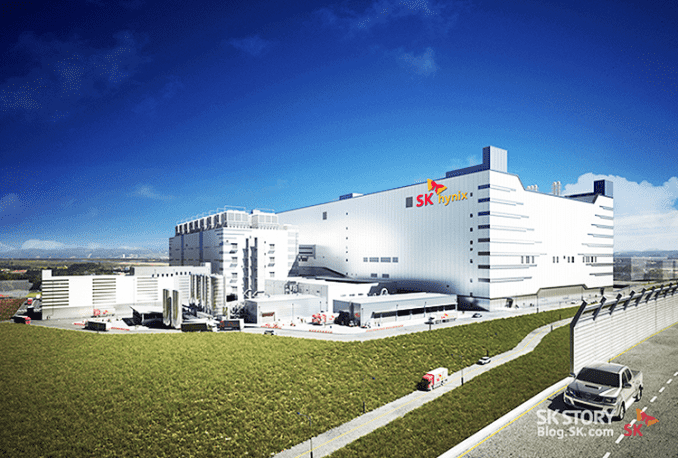
As reported earlier, SK Hynix also plans to start using the upper floor of its M14 facility to produce NAND memory this year. The company this week confirmed the plan, but revealed no specifics.

In any case, as the manufacturer continues to ramp up the M14 fab and its NAND flash output is increasing. Since SK Hynix is also gradually switching to 256 Gb (and 512 Gb starting from Q4), its NAND bit output is also gradually growing, which enables it to sell higher-capacity storage solutions.
SK Hynix also plans to start cleanroom expansion of the C2 fab in Wuxi, China, which will cost the company around $790 million and will take nearly two years. The C2 manufacturing facility is used to make DRAM and since manufacturing technologies involve more complex and lengthening production cycles, the cleanroom expansion will enable SK Hynix to maintain the current output of the C2 into the future. Keep in mind that the work is expected to be finished in April 2019, so do not expect the expansion to have any short-term effects on memory prices.
Related Reading:
- SK Hynix to Build a New NAND Fab, Upgrade Existing DRAM Fab
- SK Hynix Announces 8 GB LPDDR4X-4266 DRAM Packages
- SK Hynix Adds HBM2 to Catalog: 4 GB Stacks Set to Be Available in Q3
- Plextor Launches S2C SSDs: 16 nm SK Hynix TLC NAND and SMI SM2258
- Micron 3D NAND Update: 2D and 3D NAND Bit Crossover, Gen 2 Hits Production


