
Researchers on the Samsung Advanced Institute of Technology (SAIT) have unveiled the invention of a brand new materials, referred to as amorphous boron nitride (a-BN), in collaboration with Ulsan National Institute of Science and Technology (UNIST) and the University of Cambridge. Published within the journal Nature, the research has the potential to speed up the appearance of the following technology of semiconductors.
2D Materials – The Key to Overcoming Scalability Challenges
Recently, SAIT has been engaged on the analysis and growth of two-dimensional (2D) supplies – crystalline supplies with a single layer of atoms. Specifically, the institute has been engaged on the analysis and growth of graphene, and has achieved groundbreaking analysis outcomes on this space akin to the event of a brand new graphene transistor in addition to a novel technique of manufacturing large-area, single-crystal wafer-scale graphene. In addition to researching and creating graphene, SAIT has been working to speed up the fabric’s commercialization.
“To enhance the compatibility of graphene with silicon-based semiconductor processes, wafer-scale graphene growth on semiconductor substrates should be implemented at a temperature lower than 400°C.” mentioned Hyeon-Jin Shin, a graphene mission chief and Principal Researcher at SAIT. “We are also continuously working to expand the applications of graphene beyond semiconductors.”
2D Material Transformed – Amorphous Boron Nitride
The newly found materials, referred to as amorphous boron nitride (a-BN), consists of boron and nitrogen atoms with an amorphous molecule construction. While amorphous boron nitride is derived from white graphene, which incorporates boron and nitrogen atoms organized in a hexagonal construction, the molecular construction of a-BN in truth makes it uniquely distinctive from white graphene.
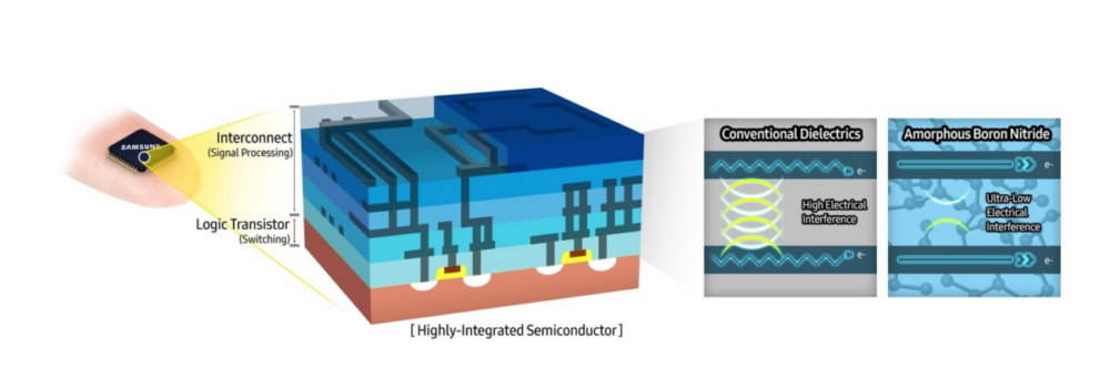
Amorphous boron nitride has a best-in-class ultra-low dielectric fixed of 1.78 with robust electrical and mechanical properties, and can be utilized as an interconnect isolation materials to reduce electrical interference. It was additionally demonstrated that the fabric will be grown on a wafer scale at a low temperature of simply 400°C. Thus, amorphous boron nitride is anticipated to be broadly utilized to semiconductors akin to DRAM and NAND options, and particularly in subsequent technology reminiscence options for large-scale servers.
“Recently, interest in 2D materials and the new materials derived from them has been increasing. However, there are still many challenges in applying the materials to existing semiconductor processes.” mentioned Seongjun Park, Vice President and Head of Inorganic Material Lab, SAIT. “We will continue to develop new materials to lead the semiconductor paradigm shift.”
2012: Graphene Barristor, a Triode Device with a Gate-Controlled Schottky Barrier (SAIT, printed in Science)
2014: Wafer-Scale Growth of Single-Crystal Monolayer Graphene on Reusable Hydrogen-Terminated Germanium (SAIT and Sungkyunkwan University, printed in Science)
2017: Realization of steady Zachariasen carbon monolayer (SAIT and Sungkyunkwan University, printed in Science Advances)
2020: Ultra-low dielectric fixed amorphous boron nitride (SAIT, UNIST and University of Cambridge, printed in Nature)


