
Industry-leading bit density with about 50% enhance in comparison with earlier technology
Productivity for the V-NAND’s groundbreaking double-stack construction enhanced by superior ‘channel hole etching’ know-how
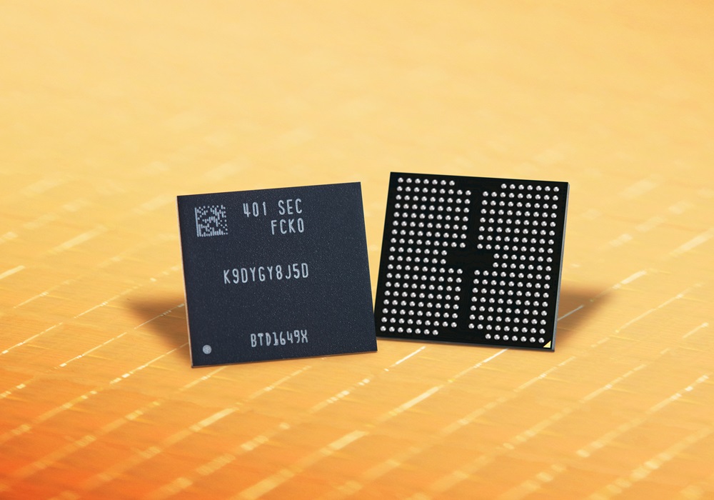
Samsung Electronics, the world chief in superior reminiscence know-how, as we speak introduced that it has begun mass manufacturing for its one-terabit (Tb) triple-level cell (TLC) Ninth-generation vertical NAND (V-NAND), solidifying its management within the NAND flash market.
“We are excited to deliver the industry’s first 9th-gen V-NAND which will bring future applications leaps forward. In order to address the evolving needs for NAND flash solutions, Samsung has pushed the boundaries in cell architecture and operational scheme for our next-generation product,” stated SungHoi Hur, Head of Flash Product & Technology of the Memory Business at Samsung Electronics. “Through our latest V-NAND, Samsung will continue to set the trend for the high-performance, high-density solid-state drive (SSD) market that meets the needs for the coming AI generation.”
With the business’s smallest cell measurement and thinnest mildew, Samsung improved the bit density of the Ninth-generation V-NAND by about 50% in comparison with the Eighth-generation V-NAND. New improvements corresponding to cell interference avoidance and cell life extension have been utilized to reinforce product high quality and reliability, whereas eliminating dummy channel holes has considerably lowered the planar space of the reminiscence cells.
In addition, Samsung’s superior “channel hole etching” know-how showcases the corporate’s management in course of capabilities. This know-how creates electron pathways by stacking mildew layers and maximizes fabrication productiveness because it allows simultaneous drilling of the business’s highest cell layer rely in a double-stack construction. As the variety of cell layers enhance, the power to pierce by increased cell numbers turns into important, demanding extra refined etching strategies.
The Ninth-generation V-NAND is provided with the next-generation NAND flash interface, “Toggle 5.1,” which helps elevated knowledge enter/output speeds by 33% to as much as 3.2 gigabits-per-second (Gbps). Along with this new interface, Samsung plans to solidify its place throughout the high-performance SSD market by increasing assist for PCIe 5.0.
Power consumption has additionally been improved by 10% with developments in low-power design, in comparison with the earlier technology. As lowering power utilization and carbon emissions turns into important for purchasers, Samsung’s Ninth-generation V-NAND is anticipated to be an optimum answer for future functions.
Samsung has began mass manufacturing for the 1Tb TLC Ninth-generation V-NAND this month, adopted by the quad-level cell (QLC) mannequin within the second half of this 12 months.


