Kicking off a really digital model of the SC20 supercomputing present, NVIDIA this morning is asserting a brand new model of their flagship A100 accelerator. Barely launched 6 months in the past, NVIDIA is getting ready to launch an up to date model of the GPU-based accelerator with 80 gigabytes of HBM2e reminiscence, doubling the capability of the preliminary model of the accelerator. And as an added kick, NVIDIA is dialing up the reminiscence clockspeeds as effectively, bringing the 80GB model of the A100 to three.2Gbps/pin, or simply over 2TB/second of reminiscence bandwidth in whole.
The 80GB model of the A100 will proceed to be offered alongside the 40GB model – which NVIDIA is now calling the A100 40GB – and it’s being primarily geared toward clients with supersized AI knowledge units. Which at face worth could sound a bit apparent, however with deep studying workloads particularly, reminiscence capability could be a strongly bounding issue when working with significantly massive datasets. So an accelerator that’s massive sufficient to maintain a whole mannequin in native reminiscence can doubtlessly be considerably sooner than one which has to incessantly go off-chip to swap knowledge.
| NVIDIA Accelerator Specification Comparison | |||||
| A100 (80GB) | A100 (40GB) | V100 | |||
| FP32 CUDA Cores | 6912 | 6912 | 5120 | ||
| Boost Clock | 1.41GHz | 1.41GHz | 1530MHz | ||
| Memory Clock | 3.2Gbps HBM2e | 2.4Gbps HBM2 | 1.75Gbps HBM2 | ||
| Memory Bus Width | 5120-bit | 5120-bit | 4096-bit | ||
| Memory Bandwidth | 2.0TB/sec | 1.6TB/sec | 900GB/sec | ||
| VRAM | 80GB | 40GB | 16GB/32GB | ||
| Single Precision | 19.5 TFLOPs | 19.5 TFLOPs | 15.7 TFLOPs | ||
| Double Precision | 9.7 TFLOPs (1/2 FP32 fee) |
9.7 TFLOPs (1/2 FP32 fee) |
7.eight TFLOPs (1/2 FP32 fee) |
||
| INT8 Tensor | 624 TOPs | 624 TOPs | N/A | ||
| FP16 Tensor | 312 TFLOPs | 312 TFLOPs | 125 TFLOPs | ||
| TF32 Tensor | 156 TFLOPs | 156 TFLOPs | N/A | ||
| Interconnect | NVLink 3 12 Links (600GB/sec) |
NVLink 3 12 Links (600GB/sec) |
NVLink 2 6 Links (300GB/sec) |
||
| GPU | GA100 (826mm2) |
GA100 (826mm2) |
GV100 (815mm2) |
||
| Transistor Count | 54.2B | 54.2B | 21.1B | ||
| TDP | 400W | 400W | 300W/350W | ||
| Manufacturing Process | TSMC 7N | TSMC 7N | TSMC 12nm FFN | ||
| Interface | SXM4 | SXM4 | SXM2/SXM3 | ||
| Architecture | Ampere | Ampere | Volta | ||
Diving proper into the specs, the one distinction between the 40GB and 80GB variations of the A100 shall be reminiscence capability and reminiscence bandwidth. Both fashions are transport utilizing a mostly-enabled GA100 GPU with 108 energetic SMs and a lift clock of 1.41GHz. Similarly, the TDPs between the 2 fashions stay unchanged as effectively. So for pure, on-paper compute throughput, there’s no distinction between the accelerators.
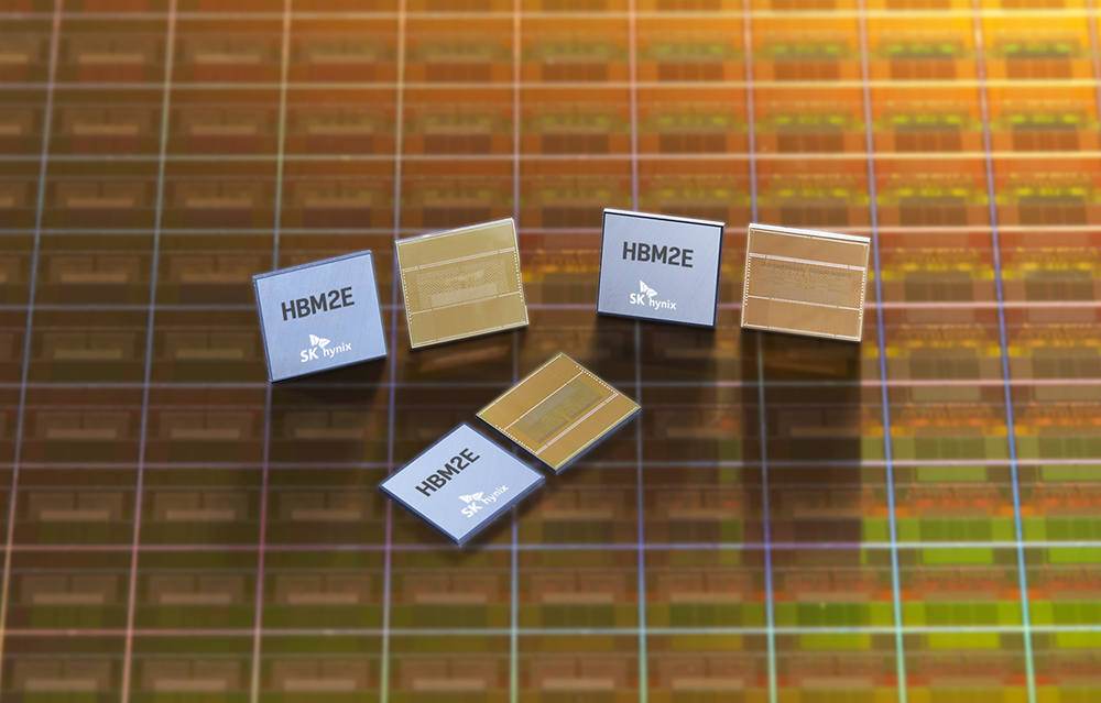
Instead, the enhancements for the A100 come right down to its reminiscence capability and its larger reminiscence bandwidth. When the unique A100 again in May, NVIDIA geared up it with six 8GB stacks of HBM2 reminiscence, with a kind of stacks disabled for yield causes. This left the unique A100 with 40GB of reminiscence and simply shy of 1.6TB/second of reminiscence bandwidth.
For the newer A100 80GB, NVIDIA is holding the identical configuration of 5-out-of-6 reminiscence stacks enabled, nevertheless the reminiscence itself has been changed with newer HBM2E reminiscence. HBM2E is the casual identify given to the latest replace to the HBM2 reminiscence normal, which again in February of this 12 months outlined a brand new most reminiscence velocity of three.2Gbps/pin. Coupled with that frequency enchancment, manufacturing enhancements have additionally allowed reminiscence producers to double the capability of the reminiscence, going from 1GB/die to 2GB/die. The internet outcome being that HBM2E provides each larger capacities in addition to larger bandwidths, two issues which NVIDIA is benefiting from right here.