
One of the guarantees that Intel has made with its new Xe GPU household is that in its varied types it’s going to cater to makes use of starting from built-in graphics all the way in which as much as the excessive efficiency compute fashions wanted for super-dense supercomputers. This means help for the sorts of calculations concerned in easy graphics, advanced graphics, ray tracing, AI inference, AI coaching, and the compute that goes into molecular modelling, oil-and-gas, nuclear reactors, rockets, nuclear rockets, and all the opposite huge questions the place extra compute provides extra capabilities. Sitting close to the highest of Intel’s choices is the Xe-HP structure, designed to supply excessive efficiency GPUs for traditional server and enterprise deployments.
Over the previous couple of weeks Intel has provided among the first technical particulars of Xe-HP, following Raja Koduri displaying it off throughout his social media profiles. We know that it’s designed to be a modular structure, with completely different chiplets linked collectively utilizing Intel’s Embedded Multi-Die Interconnect Bridge expertise. We additionally know, because of disclosures made at Intel’s Architecture Day, that it’s set to be constructed on Intel’s 10nm Enhanced SuperFin (10ESF, previously 10++, previously 10+++) manufacturing course of, which we imagine to be a late 2021 course of. Raja Koduri promised through the Architecture Day presentation that Xe-HP (and Xe-HPG) shall be obtainable in 2021.

Intel defined that the modular Xe-HP design will scale from one to 4 tiles, and the idea of Xe-HP was to ‘scale everything’, resembling execution models, frequency, bandwidth, IPC, and math capabilities. We assume that every tile could have direct entry to some on-chip reminiscence as properly – actually scaling up each side of a chip – though how the chip’s HBM2E is allotted hasn’t been confirmed. The level of the product is that it’s designed for the data-center, so there must be a mixture of media compute in addition to uncooked compute, protecting all types of makes use of instances.

As a part of the demonstration throughout Architecture Day, Intel additionally showcased that they’ve been working some benchmarks on the early silicon within the labs. By early silicon, we imply that these aren’t working on the closing frequencies, this isn’t closing firmware, and the software program stack nonetheless has a solution to go, so undoubtedly there are optimizations at each stage.

First, Intel confirmed {that a} single tile of Xe-HP can’t solely transcode one 4K60 video in actual time, however ten. In the demonstration they’d the FFmpeg output, displaying that the demo was changing every video from 5332 kb/s general all the way down to 3000 kb/s common (6000 kb/s max).
For compute, Intel provided the next efficiency numbers, given as peak GFLOPs of FP32 math utilizing the OpenCL-based CLPeak benchmark.
- One Tile: 10588 GFLOPs (10.6 TF) of FP32
- Two Tile: 21161 GFLOPs (21.2 TF) of FP32 (1.999x)
- Four Tile: 42277 GFLOPs (42.Three TF) of FP32 (3.993x)
We additionally get some further data from the video of Xe-HP. The assessments had been finished on Linux, and truly all finished on a model of the quad-tile chip, however made to run in 1T/2T/4T modes. This is why when trying on the video we will see all three variations are working at 1300 MHz. The string used for the chip is ‘XeHP HD Graphics NEO’ as properly.
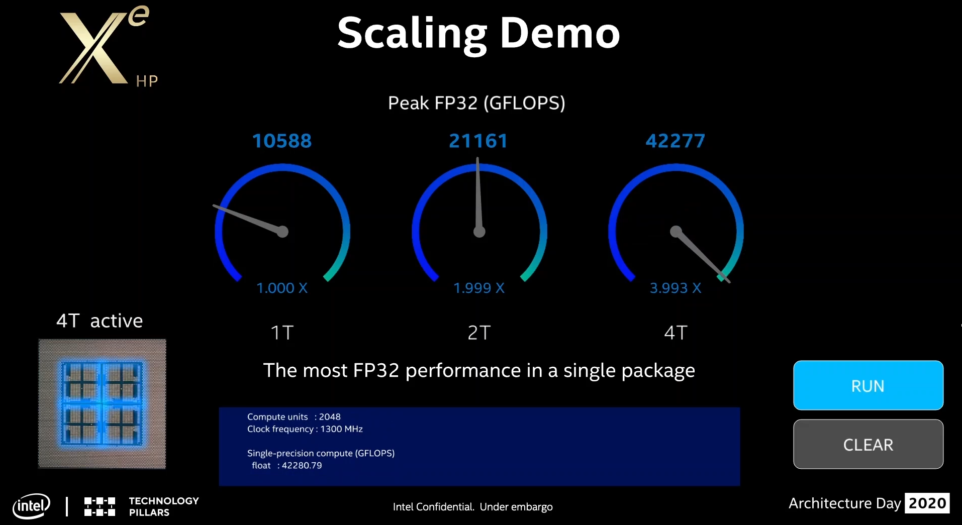
The video additionally reveals {that a} single tile has 512 ‘compute units’, whereas the twin tile has 1024 compute models and the quad-tile has 2048 compute models. And whereas Intel hasn’t formally claried what “compute units” imply on this context, the efficiency figures all however affirm that it is counting Intel’s Execution Units. Based on the given GFLOPs, the acknowledged clock velocity, and the Xe structure’s eight pipes per Execution unit with twin FMAs, Intel’s efficiency figures map to 512/1024/2048 EUs respectively….


