
Apparently, “Rocket Lake-S” is a multi-chip module of a 14 nm die that holds the CPU cores; and 10 nm die that holds the uncore elements. AMD “Matisse” and “Vermeer” too have such a division of labor, however the CPU cores are situated on dies with a extra superior silicon fabrication course of (7 nm), than the die with the uncore elements (12 nm).
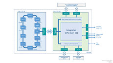
The 14 nm CPU die on “Rocket Lake-S” holds “Willow Cove” CPU cores which are presupposed to introduce important IPC positive factors over “Skylake.” In this die, there are CPU cores and a reduced-functionality system agent, that are sure collectively by a Ring-bus interconnect. This system agent talks to its counterpart on the uncore die (aka “GPU die”), over EMIB interconnect.
The 10 nm GPU die (aka uncore die) options the processor’s Gen12 Xe iGPU with as much as 96 execution models, a dual-channel DDR4 reminiscence controller, and a PCI-Express 4.zero root-complex, in addition to different minor elements associated to the iGPU, corresponding to its display- and media engines.
Unlike each previous Intel mainstream desktop technology since “Lynnfield,” the “Rocket Lake-S” MCM places out a complete of 24 PCI-Express lanes. 16 of those are assigned as PEG (PCI-Express Graphics, or the principle PCI-Express x16 slot on the platform); and eight lanes are assigned as chipset bus. In previous microarchitectures, together with “Comet Lake-S,” the processor solely put out 20 lanes, 16 of that are towards PEG, and Four towards the chipset-bus (DMI).
This will not be the primary time that Intel took the MCM method in its mainstream desktop processors. The first technology “Clarkdale” desktop processor within the LGA1156 package deal was an MCM of a 32 nm CPU die, and a 45 nm uncore die (which contained the iGPU).
Why Intel selected to present the iGPU, reasonably than the CPU cores, the benefit of the extra superior silicon fabrication course of is a thriller that can solely be solved after launch. Perhaps it is merely not attainable to construct a Gen12 iGPU on 14 nm, whereas the effectivity of “Willow Cove” CPU cores, initially designed for 10 nm+, can survive a back-port to 14 nm higher. “Willow Cove” cores make their debut with the “Tiger Lake-U” cell processors.


