
An government visiting numerous analysis divisions throughout the globe isn’t essentially new, however with a concentrate on social media driving named people at every firm to maintain their followers sitting on the sting of their seats signifies that we get much more insights into how these corporations function. The draw back of posting to social media is when sure photos exposing unreleased data aren’t vetted by PR or authorized, and we get a glimpse into the following era of know-how. That is what occurred as we speak.
Day 1 with the @intel Israel crew within the books. Great views…unimaginable opp to see @GetThunderbolt innovation …a validation lab tour and time with the crew…can’t wait to see what tomorrow brings! pic.twitter.com/GKOddA6TNi
— Gregory M Bryant (@gregorymbryant) August 1, 2021
EVP and GM of Intel’s Client Computing Group, Gregory Bryant, is that this week spending a while at Intel’s Israel R&D amenities in his first abroad Intel journey in of 2021. An early submit on Sunday morning, showcasing Bryant’s journey to the gymnasium to beat jetlag, was adopted by one other later within the day with Bryant being proven the places of work and the analysis. The submit contained 4 images, however was quickly deleted and changed by a photograph with three (within the tweet above). The picture eliminated showcases some new details about next-generation Thunderbolt know-how.
In this picture we will see a poster on the wall showcasing ‘80G PHY Technology’, which signifies that Intel is engaged on a bodily layer (PHY) for 80 Gbps connections. Off the bat that is double the bandwidth of Thunderbolt 4, which runs at 40 Gbps.
The second line confirms that that is ‘USB 80G is focused to assist the present USB-C ecosystem’, which follows alongside that Intel is aiming to keep up the USB-C connector however double the efficient bandwidth.
The third line is definitely the place it will get technically fascinating. ‘The PHY might be primarily based on novel PAM-Three modulation know-how’. This is speaking about how the Zero and 1s are transmitted – historically we discuss NRZ encoding, which simply permits for a Zero or a 1 to be transmitted, or a single bit. The pure development is a scheme permitting two bits to be transferred, and that is referred to as PAM-4 (Pulse Amplitude Modulation), with the Four being the demarcation for what number of totally different variants two bits may very well be seen (both as 00, 01, 10, or 11). PAM-4, on the similar frequency, thus has 2x the bandwidth of an NRZ connection.
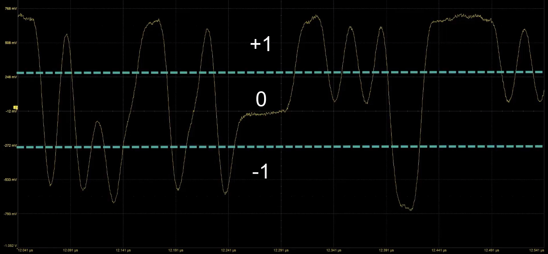
So what on earth in PAM-3?
From Teledyne LaCroy on YouTube
PAM-Three is a know-how the place the info line can carry both a -1, a 0, or a +1. What the system does is definitely mix two PAM-Three transmits right into a 3-bit knowledge sign, equivalent to 000 is an -1 adopted by a -1. This will get complicated, so here’s a desk:
| PAM-3 Encoding | ||
| AnandTech | Transmit 1 |
Transmit 2 |
| 000 | -1 | -1 |
| 001 | -1 | 0 |
| 010 | -1 | 1 |
| 011 | 0 | -1 |
| 100 | 0 | 1 |
| 101 | 1 | -1 |
| 110 | 1 | 0 |
| 111 | 1 | 1 |
| Unused | 0 | 0 |
When we examine NRZ to PAM-Three and PAM-4, we will see the speed of information switch for PAM-Three is in the course of NRZ and PAM-4. The motive why PAM-Three is getting used on this case is to attain that larger bandwidth with out the additional limitations that PAM-Four requires to be enabled.
| NRZ vs PAM-Three vs PAM4 | |||
| AnandTech | Bits | Cycles | Bits Per Cycle |
| NRZ | 1 | 1 | 1 |
| PAM-3 | 3 | 2 | 1.5 |
| PAM-4 | 2 | 1 | 2 |
PAM-3 has related limitations to NRZ.

The ultimate line on this picture is ‘[something] N6 test-chip specializing in the brand new PHY know-how is working in [the lab and] exhibiting promising outcomes’. That first phrase I assumed was TSMC, nevertheless it needs to be about the identical width because the ‘The’ on the road above. So it doesn’t…


 for ChatGPT, G…")

