
As a results of being on the US Entity checklist, SMIC's blacklisting has precipitated troubles within the firm creating and deploying modern fabrication applied sciences. As a end result, it has been pressured to concentrate on mature nodes, which nonetheless have loads of use in long-life cycle components for electronics and the automotive trade. On Friday the corporate introduced plans to construct China's first GigaFab, a 300 mm manufacturing facility with deliberate capability of round 100,000 wafer begins per thirty days (WSPM). The fab will price almost $8.87 billion.
Building Up Capacity for Mature Nodes
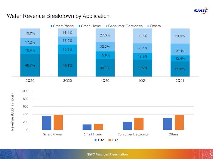
The new fab shall be positioned close to Shanghai, within the Lingang Free Trade Zone (FTZ), and shall be constructed as a partnership between SMIC and the Shanghai Municipal People’s Government. The fab will course of 300 mm wafers utilizing mature manufacturing applied sciences, corresponding to 28 nm and above. These nodes are sometimes used for numerous chips with a really lengthy lifecycle, and that are in brief provide now. Over the previous few months numerous main PC makers complained about deficit of low cost elements like show driver ICs (DDICs) or Wi-Fi controllers and these chips are made utilizing 28 nm and bigger nodes. Other industries, such because the automotive trade, have been crying out for brand new provides – given China's quite massive automotive market, there may be pent up demand for extra sources of elementary digital elements.
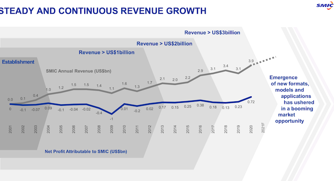
SMIC didn’t point out when it expects the brand new fab to go surfing, however it’s affordable to count on it to develop into operational two or three years down the highway. Despite this the corporate additionally didn’t enhance its CapEx of $4.three billion for 2021 from the quantity it introduced earlier this yr, maybe indiciating that this shall be a 2022 mission when it begins. Once this occurs, SMIC will be capable to make a major contribution to the worldwide provide of semiconductors produced utilizing mature fabrication processes.
The new fab shall be China's solely GigaFab for logic semiconductors (it has a number of for DRAM, which is taken into account separate). Here we’re utilizing TSMC's terminology for 'GigaFab', which is a 300mm fab with a manufacturing capability of 100,000 or extra wafer begins per month.
Earlier this yr SMIC initiated a mission to construct a 300mm fab close to Shenzhen for $2.35 billion. That fab is about to ultimately obtain manufacturing capability of round 40,000 wafer begins per thirty days and use 28 and bigger fabrication applied sciences. This smaller fab will begin operations generally in 2022, as semiconductor capability demand by native corporations in China is rising.
In a bid to equip each fabs, SMIC inevitably has to make use of gear produced by the U.S.-based makers, corresponding to Applied Materials, Lam Research, KLA, and Axcelis. All of them utilized for export licenses to produce SMIC for the reason that foundry is in the U.S. Department of Commerce's Entity List earlier this yr. While we have no idea in the event that they had been granted, the actual fact that SMIC declares a fab with an unprecedented capability (for China and SMIC) signifies that it believes it will probably equip its manufacturing amenities with correct gear, both from the US or elsewhere.
As all the time, SMIC will share possession of the fab with authorities, on this particular case within the Lingang Free Trade Zone with co-investors. SMIC will personal a controlling 51% stake, Shanghai Municipal People’s Government will personal much less than 25% and the excellent 24% shall be managed by different buyers set to be 'mutually discovered by SMIC and the native authorities.'
Just In Time
Mature course of applied sciences, corresponding to 40/45 nm, 55/65 nm, and 150/180 nm have been SMIC's livelihood, so increasing capacities for 300mm primarily based processes (something from 28nm to 45nm – bigger course of nodes are typically on 200mm wafers) makes an incredible sense for the corporate. Furthermore, the corporate is…

