
Advanced system-on-chip designs are extraordinarily advanced by way of transistor depend and are exhausting to construct utilizing the most recent fabrication processes. In a bid to make manufacturing of next-generation chips economically possible, chip fabs want to make sure excessive yields early of their lifecycle by shortly discovering and correcting defects.
But discovering and fixing defects will not be straightforward as we speak, as conventional optical inspection instruments do not provide sufficiently detailed picture decision, whereas high-resolution e-beam and multibeam inspection instruments are comparatively sluggish. Looking to bridge the hole on inspection prices and time, Applied Materials has been growing a know-how referred to as ExtractAI know-how, which makes use of a mixture of the corporate’s newest Enlight optical inspection software, SEMVision G7 e-beam overview system, and deep studying (AI) to shortly discover flaws. And surprisingly, this answer has been in use for a couple of 12 months now.
“Applied’s new playbook for process control combines Big Data and AI to deliver an intelligent and adaptive solution that accelerates our customers’ time to maximum yield,” stated Keith Wells, group vp and normal supervisor, Imaging and Process Control at Applied Materials. “By combining our best-in-class optical inspection and eBeam review technologies, we have created the industry’s only solution with the intelligence to not only detect and classify yield-critical defects but also learn and adapt to process changes in real-time. This unique capability enables chipmakers to ramp new process nodes faster and maintain high capture rates of yield-critical defects over the lifetime of the process.”
Defect Detection: A Crucial Step in Chip Manufacturing
As a extremely aggressive trade, the semiconductor trade can be extraordinarily time delicate. Modern corporations must develop new chips, bug repair them, after which launch all of them on pretty tight schedules. Nowadays it takes years to develop a complicated chip and a number of other months to really fabricate a batch. One of essentially the most essential time parameters is time to yield, which is to say with the ability to present a lot of chips with excessive sufficient yields. A chip designer might have essentially the most environment friendly structure round, but when they can’t get it made in excessive volumes, they will nonetheless lose out on cash and market share. Even foundries really feel this pinch, because the time wanted to repair defects and produce traces as much as snuff represents tens of millions of {dollars} in tools depreciation alone – one week of a 3nm fab downtime is anticipated to price $25 million in unamortized depreciation prices. So attaining acceptable time to yield metrics closely is determined by a fab’s capacity to detect and repair yield-killing defects.
Since the vast majority of superior SoCs are made utilizing extraordinarily small fabrication processes – a lot of which depend on multi patterning and/or excessive ultraviolet (EUV) lithography – it’s getting very robust to detect defects. Applied Materials says that the variety of course of steps elevated by 48% from 2015 to 2021.
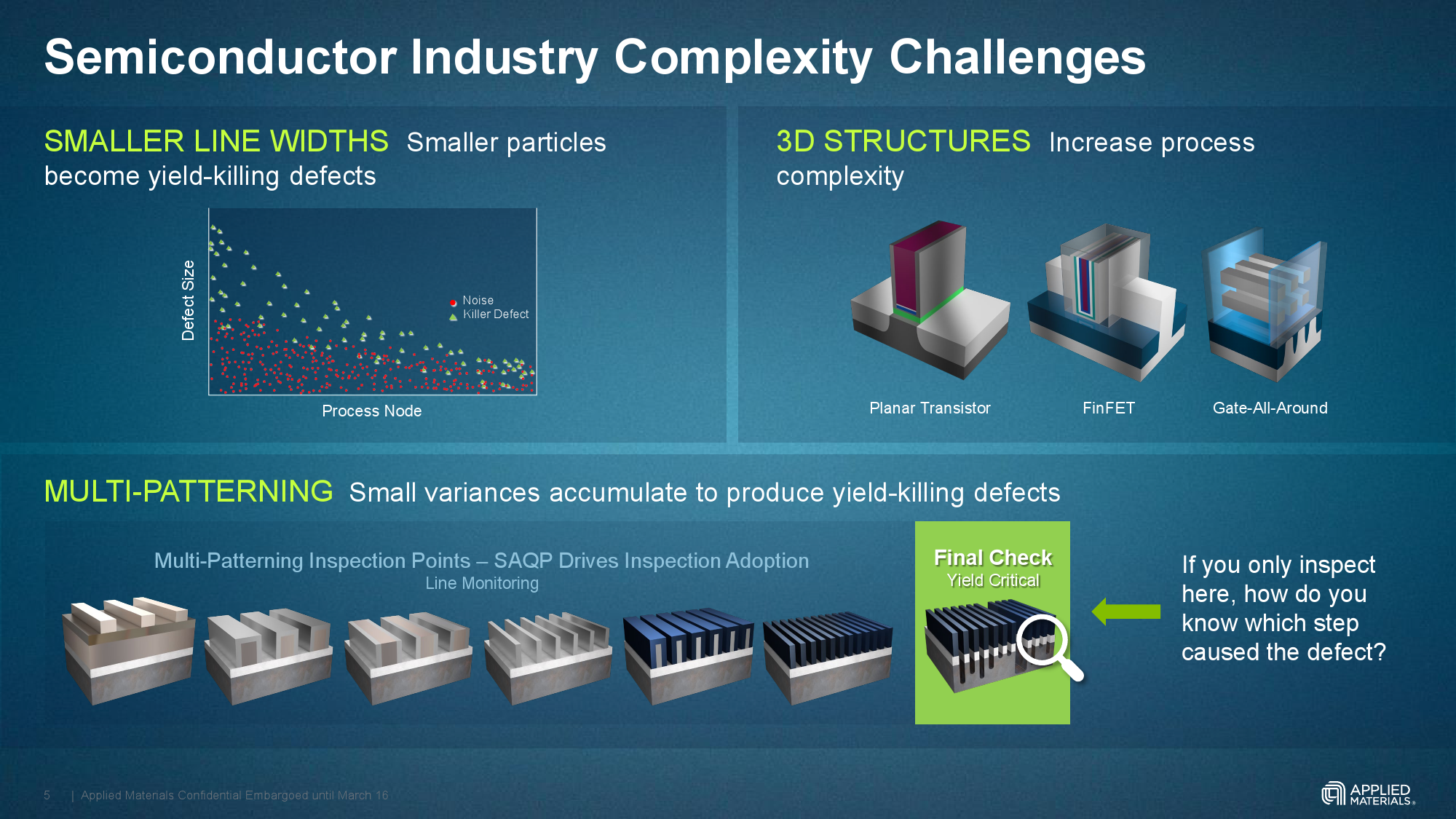
Meanwhile, small variances and line widths can find yourself as yield-killing defects in the event that they multiply. Furthermore, if these tiny variances are detected late, all the method steps made after the variance was launched are basically wasted money and time. In reality, even late detection could be thought-about unhealthy luck, as monitoring down the foundation reason behind a defect of an IC that includes FinFET transistors and made utilizing multi patterning is extraordinarily exhausting.
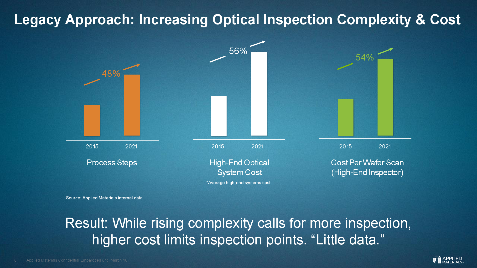
Just like scanners used to construct chips, inspection instruments have developed considerably over time. But additionally they have change into dearer, which will increase price per wafer scan. According to Applied Materials, the worth tag on a high-end optical inspection system has elevated by 56% within the final six years, which in…


