
As the world transitions to a low-carbon energy future, near-term, large-scale deployment of solar power will be critical to mitigating climate change by midcentury. Climate scientists estimate that the world will need 10 terawatts (TW) or more of solar power by 2030 — at least 50 times the level deployed today. At the MIT Photovoltaics Research Laboratory (PVLab), teams are working both to define what’s needed to get there and to help make it happen. “Our job is to figure out how to reach a minimum of 10 TW in an economically and environmentally sustainable way through technology innovation,” says Tonio Buonassisi, associate professor of mechanical engineering and lab director.
Their analyses outline a daunting challenge. First they calculated the growth rate of solar required to achieve 10 TW by 2030 and the minimum sustainable price that would elicit that growth without help from subsidies. Current technology is clearly not up to the task. “It would take between $1 trillion and $4 trillion of additional debt to just push current technology into the marketplace to do the job, and that’d be hard,” says Buonassisi. So what needs to change?
Using models that combine technological and economic variables, the researchers determined that three changes are required: reduce the cost of modules by 50 percent, increase the conversion efficiency of modules (the fraction of solar energy they convert into electricity) by 50 percent, and decrease the cost of building new factories by 70 percent. Getting all of that to happen quickly enough — within five years — will require near-term policies to incentivize deployment plus a major push on technological innovation to reduce costs so that government support can decrease over time.
Making strides on efficiency
Major gains are already being made on the conversion efficiency front — both at the MIT PVLab and around the world. One especially promising technology is the passivated emitter and rear cell (PERC), which is based on low-cost crystalline silicon but has a special “architecture” that captures more of the sun’s energy than conventional silicon cells do. While costs must be brought down, the technology promises to bring a 7 percent increase in efficiency, and many experts predict its widespread adoption.
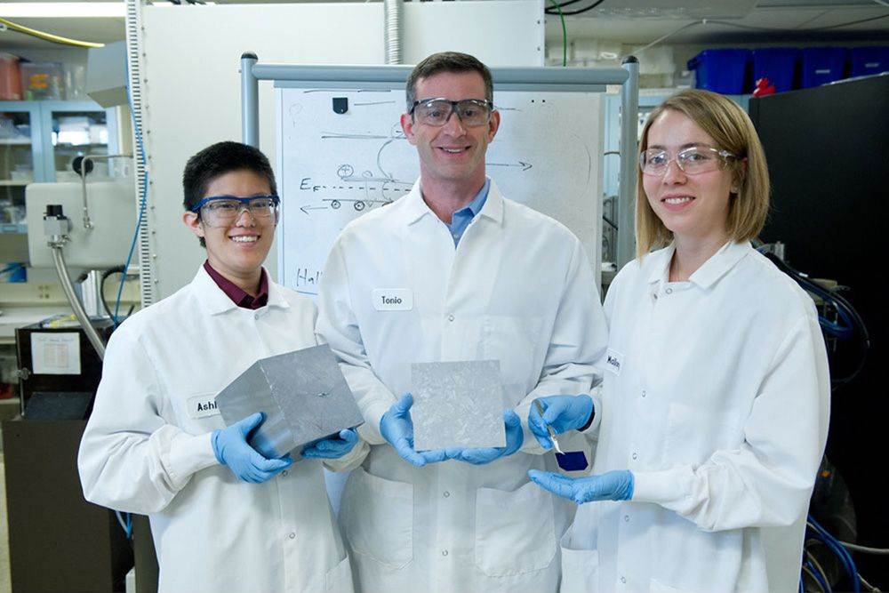
But there’s been a problem. In field tests, some modules containing PERC solar cells have degraded in the sun, with conversion efficiency dropping by fully 10 percent in the first three months. “These modules are supposed to last 25 years, and within just weeks to months they’re generating only 90 percent as much electricity as they’re designed for,” says Ashley Morishige, postdoc in mechanical engineering. That behavior is perplexing because manufacturers thoroughly test the efficiency of their products before releasing them. In addition, not all modules exhibit the problem, and not all companies encounter it. Interestingly, it took up to a few years before individual companies realized that other companies were having the same problem. Manufacturers came up with a variety of engineering solutions to deal with it, but its exact cause remained unknown, prompting concern that it could recur at any time and could affect next-generation cell architectures.
To Buonassisi, it seemed like an opportunity. His lab generally focuses on basic materials problems at the wafer and cell level, but the researchers could equally well apply their equipment and expertise to modules and systems. By defining the problem, they could support the adoption of this energy-efficient technology, helping to bring down materials and labor costs for each watt of power generated.
Working closely with an industrial solar cell manufacturer, the MIT team undertook a “root-cause analysis” to define the source of the problem. The company had come to them for help with the unexpected degradation of their PERC modules and reported some odd trends. PERC modules stored in sunlight for 60 days with their wires connected into a closed loop lost no more efficiency than conventional solar cells typically do during their break-in period. But modules stored in sunlight with open circuits degraded significantly more. In addition, modules made from different silicon ingots displayed different power-loss behavior. And, as shown in Figure 1 in the slideshow above, the drop in efficiency was markedly higher in modules made with cells that had been fabricated at a peak temperature of 960 degrees Celsius than in those containing cells fired at 860 C.
Subatomic misbehavior
Understanding how defects can affect conversion efficiency requires understanding how solar cells work at a fundamental level. Within a photoreactive material such as silicon, electrons exist at two distinct energy levels. At the lower level, they’re in the “valence band” and can’t flow; at the higher level, they’re in the “conduction band” and are free to move. When solar radiation shines onto the material, electrons can absorb enough energy to jump from the valance band to the conduction band, leaving behind vacancies called holes. If all is well, before the electrons lose that extra energy and drop back to the valence band, they travel through an external circuit as electric current.
Generally, an electron or hole has to gain or lose a set amount of energy to move from one band to the other. (Although holes are defined as the absence of electrons, physicists view both electrons and holes as “moving” within semiconductors.) But sometimes a metal impurity or a structural flaw in the silicon provides an energy “state” between the valence and conduction bands, enabling electrons and holes to jump to that intermediate energy level — a move achieved with less energy gain or loss. If an electron and hole both make the move, they can recombine, and the electron is no longer available to pass through the external circuit. Power output is lost.
The PVLab researchers quantify that behavior using a measure called lifetime — the average time an electron remains in an excited state before it recombines with a hole. Lifetime critically affects the energy conversion efficiency of a solar cell, and it is “exquisitely sensitive to the presence of defects,” says Buonassisi.
To measure lifetime, the team — led by Morishige and mechanical engineering graduate student Mallory Jensen — uses a technique called lifetime spectroscopy. It involves shining light on a sample or heating it up and monitoring electrical conductivity during and immediately afterward. When current flow goes up, electrons excited by the added energy have jumped into the conduction band. When current drops, they’ve lost that extra energy and fallen back into the valence band. Changes in conductivity over time thus indicate the average lifetime of electrons in the sample.
Locating and characterizing the defect
To address the performance problems with PERC solar cells, the researchers first needed to figure out where in the modules the primary defects were located. Possibilities included the silicon surface, the aluminum backing, and various interfaces between materials. But the MIT team thought it was likely to be in the bulk silicon itself.
To test that assumption, they used partially fabricated solar cells that had been fired at 750 C or at 950 C and — in each category — one that had been exposed to light and one that had been kept in the dark. They chemically removed the top and bottom layers from each cell, leaving only the bare silicon wafer. They then measured the electron lifetime of all the samples. As shown in Figure 2 in the slideshow above, with the low-temperature pair, lifetime is about the same in the light-exposed and unexposed samples. But with the high-temperature pair, lifetime in the exposed sample is significantly lower than that in the unexposed sample.
Those findings confirm that the observed degradation is largely attributable to defects that are present in the bulk silicon and — when exposed to light — affect lifetime, thus conversion efficiency, in cells that have been fired at higher temperatures. In follow-up tests, the researchers found that by reheating the degraded samples at 200 C for just an hour, they could bring the lifetime back up — but it dropped back down with re-exposure to light.
So how do those defects interfere with conversion efficiency, and what types of contaminants might be involved in their formation? Two characteristics of the defects would help the researchers answer those questions. First is the energy level of the defect — where it falls between the valence and conduction bands. Second is the “capture cross section,” that is, the area over which a defect at a particular location can capture electrons and holes. (The area might be different for electrons than for holes.)
While those characteristics can’t easily be measured directly in the samples, the researchers could use a standard set of equations to infer them based on lifetime measurements taken at different illumination intensities and test temperatures. Using samples that had been fired at 950 C and then exposed to light, they ran lifetime spectroscopy experiments under varying test conditions. With the gathered data, they calculated the energy level and capture cross section of the primary defect causing recombination in their samples. They then consulted the literature to see what elements are known to exhibit those characteristics, making them likely candidates for causing the drop in conversion efficiency observed in their samples.
According to Morishige, the team has narrowed down the list of candidates to a handful of possibilities. “And at least one of them is consistent with much of what we’ve observed,” she says. In this case, a metal contaminant creates defects in the crystal lattice of the silicon during fabrication. Hydrogen atoms that are present combine…


