
At the Flash Memory Summit this week, Western Digital announced that it intends to use 3D Resistive RAM (ReRAM) as storage class memory (SCM) for its future special-purpose ultra-fast SSDs. The company did not reveal any actual timelines for appropriate products, nor their specifications. However, what is important is the fact that Western Digital decided to use SanDisk’s long-discussed ReRAM along with 3D manufacturing tech to build the aforementioned special-purpose SSDs.
The amount of data that the world produces totals several zettabytes per year, which creates two challenges for the high-tech industry: one is to store the vast amounts of data more or less cost-efficiently, another is to process this data efficiently from power consumption point of view. Modern SSDs and HDDs can store plenty of information (10 to 15 TB for top-of-the-range models) and modern CPUs can process a lot of data due to increasing number of cores. However, delivering the right data to those cores poses further challenges: if the necessary data is located on an HDD/SSD, fetching them from there takes a lot of time on computer timescales (e.g., 100,000 – 10,000,000 ns) and consumes a lot of energy. Meanwhile, increasing the amount of DRAM per server is not always feasible from economic point of view.
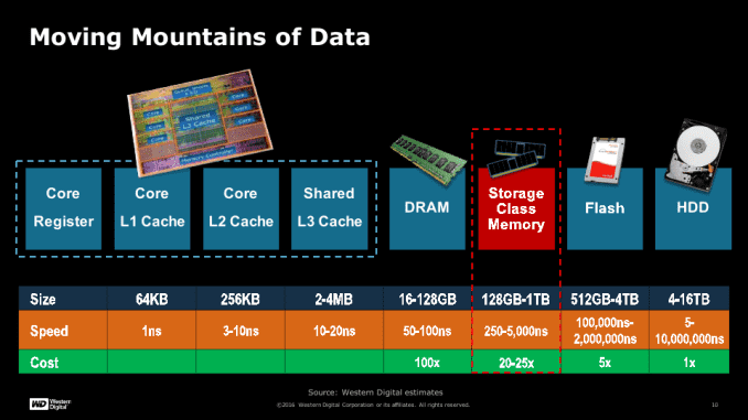
To address the challenge, the industry came up with idea of non-volatile SCM, which would sit between DRAM and storage devices and deliver much greater performance, endurance and lower latency (e.g., 250 – 5,000 ns) than NAND while costing a lot less than DRAM in terms of per-GB prices. Historically, different companies demonstrated various types of memory, which could be used as SCM (originally, this class of devices was classified as a replacement tech for NAND flash), including conductive-bridging RAM (CBRAM), phase-change memory (PCM), magnetoresistive RAM (MRAM), resistive RAM (ReRAM) and some others. All of these technologies have their own peculiarities like performance and costs (and none of them could beat NAND in terms of per-GB cost), but SanDisk has been working for years on bringing ReRAM to the market.
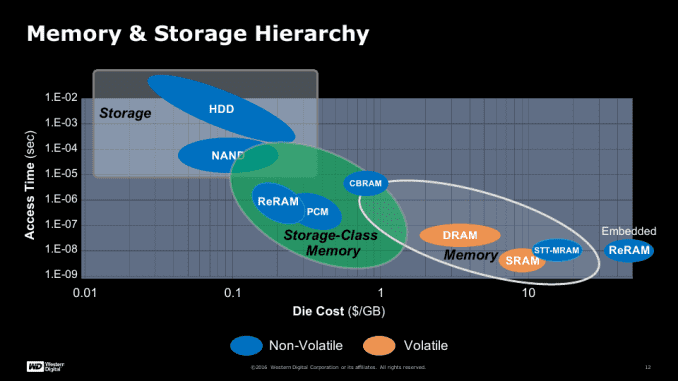
Fundamentally, ReRAM (also sometimes called RRAM) works by changing the resistance across a dielectric material by electrical current (which is why 3D XPoint is considered as a proprietary implementation of ReRAM). The resistance can be measured and considered as “0” or “1”. On paper, the technology enables higher performance and endurance when compared to NAND flash, but finding the right materials and architecture for ReRAM has taken engineers many years.
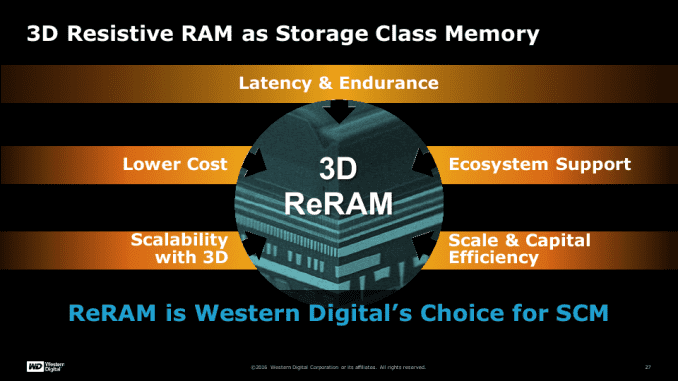
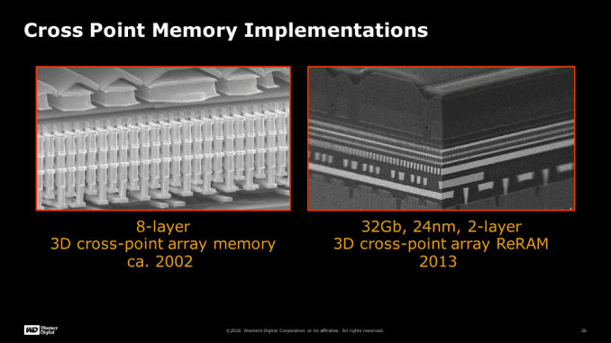
Without making any significant announcements this week, Western Digital indicated that it would use some of the things it has learnt while developing its BiCS 3D NAND to produce its ReRAM chips. The company claims that its ReRAM will feature a multi-layer cross-point implementation, something it originally revealed a while ago.
Perhaps, the most important announcement regarding the 3D ReRAM by Western Digital is the claim about scale and capital efficiency of the new memory. Essentially, this could mean that the company plans to use its manufacturing capacities as well as its infrastructure (testing, packaging, etc.) in Yokkaichi, Japan, to make 3D ReRAM. Remember that SCM is at this point more expensive than NAND, hence, it makes sense to continue using the current fabs and equipment to build both types of non-volatile memory so ensure that the SCM part of the business remains profitable. IMFT does the same thing with its SCM: it uses its fab in Lehi, Utah, to produce 3D XPoint memory, but does not reveal specifics about the process technology (just like Western Digital). Of course, Western Digital could re-use some of the fundamental technologies, materials and process architecture both for ReRAM and NAND, but the company does not any particular details on the matter just now.
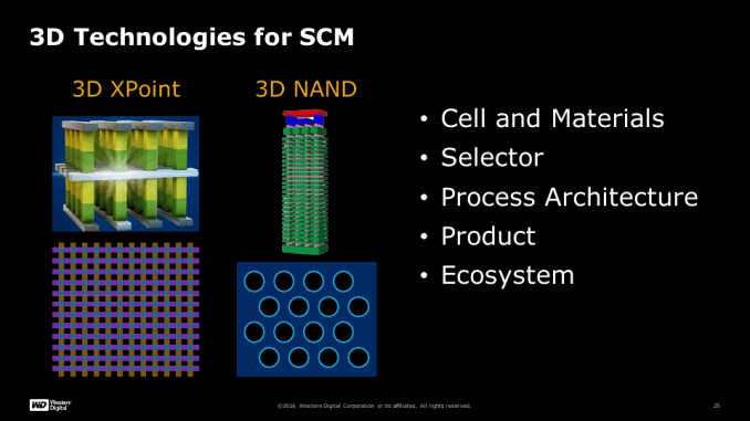
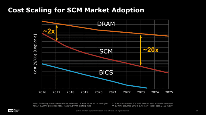
Quite naturally, WD’s 3D ReRAM will scale in terms of per-IC densities with the increase of the number of layers, though, we do not know how many layers will initial 3D ReRAM ICs from Western Digital incorporate. However, the company seems to be very optimistic about scaling of its SCM and believes that over time it will close the gap in terms of per-GB cost with BiCS NAND and will thus widen the gap with DRAM, which will make it more economically feasible.
Finally, the manufacturer said that its 3D ReRAM is already supported by the ecosystem, which means that the first SSDs based on the technology will probably use industry-standard interfaces (e.g. NVDIMM), which is not surprising. Perhaps, it also means that Western Digital is also already working with software developers to ensure that applications can take advantage of SCM in general, but we cannot confirm this at this time.
To sum up, Western Digital has finished development of ReRAM, which SanDisk has been discussing for several years now. The company plans to release actual products based on ReRAM in the foreseeable future (12 – 24 months from now, call it a guess) and to use the same fab and equipment to build ReRAM and NAND ICs. Western Digital’s ReRAM has a roadmap for the future. What remains to be seen is what is going to happen to the joint development of SCM announced by SanDisk and HP in October, 2016.
