
TSMC’s 3D-stacked system-on-integrated chips (SoIC) superior packaging applied sciences is ready to evolve quickly. In a presentation on the firm’s current expertise symposium, TSMC outlined a roadmap that can take the expertise from a present bump pitch of 9μm all the way in which all the way down to a 3μm pitch by 2027, stacking collectively combos of A16 and N2 dies.
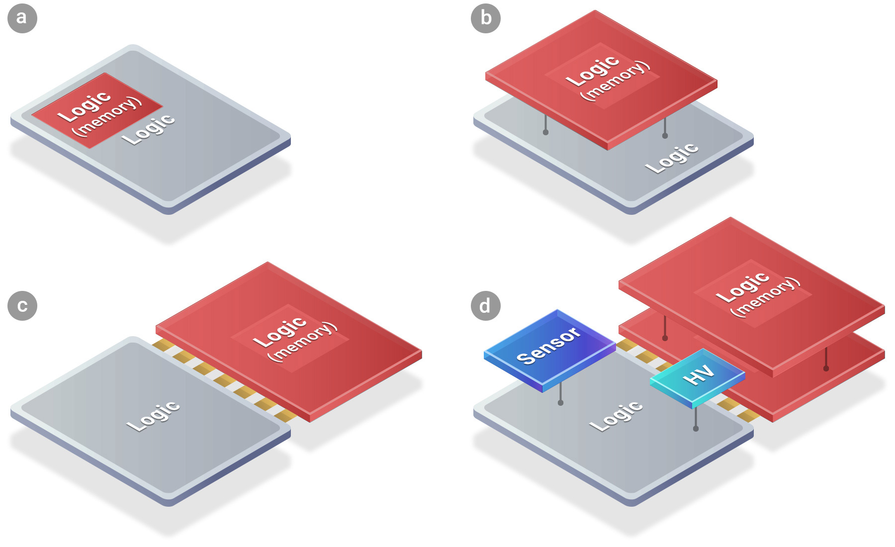
TSMC has quite a few superior packaging applied sciences, together with 2.5D CoWoS and a couple of.5D/3D InFO. Perhaps probably the most intriguing (and complicated) methodology is their 3D-stacked system-on-integrated chips (SoIC) expertise, which is TSMC’s implementation of hybrid wafer bonding. Hybrid bonding permits two superior logic units to be stacked immediately on high of one another, permitting for ultra-dense (and ultra-short) connections between the 2 chips, and is primarily geared toward excessive efficiency elements. For now, SoIC-X (bumpless) is used for choose purposes, resembling AMD’s 3D V-cache expertise for CPUs, in addition to their Instinct MI300-series AI merchandise. And whereas adoption is rising, the present technology of the expertise is constrained by limitations on die sizes and interconnection pitches.
But these limitations are anticipated to provide manner shortly, if all goes in line with plan for TSMC. SoIC-X expertise goes to advance quick, and by 2027, it will likely be doable assemble a chip pairing a reticle-sized high die made on TSMC’s modern A16 (1.6nm-class) on a backside die produced utilizing TSMC’s N2 (2nm-class). These dies, in flip, can be linked utilizing 3μm bond pitche ssilicon vias (TSVs), thrice the density of the dimensions of at the moment’s 9μm pitch. Such small interconnections will permit for a a lot bigger variety of connections general, tremendously rising the bandwidth density (and thus efficiency) of the assembled chip.
| TSMC’s SoIC-X Roadmap Data by TSMC (Compiled by AnandTech) |
||||||||
| 2022 | 2023 | 2024 | 2025 | 2026 | 2027 | |||
| Top Die | N7 | N5 | N4 | N4 | N2 | A16 | ||
| Bottom Die | N7 | ≥N6 | ≥N5 | ≥N4 | ≥N3 | ≥N2 | ||
| Bond Pitch | 9 μm | 9 μm | 6 μm | 6 μm | 4.5 μm | three μm | ||
| Size* | 0.1 reticle | 0.Four reticle | 0.eight reticle | 1 reticle | 1 reticle | 1 reticle | ||
*TSMC considers reticle measurement as roughly 830 mm2.
Improved hybrid bonding strategies are meant to permit TSMC’s huge HPC prospects – AMD, Broadcom, Intel, NVIDIA, and the like – to construct giant, ultra-dense disaggregated processor designs for demanding purposes, the place distance between the dies is important, as is the general ground area used. Meanwhile, for purposes the place solely efficiency issues, it will likely be doable to position a number of SoIC-X packages on a CoWoS interposer to get improved efficiency at a decrease energy consumption.
In addition to creating its bumpless SoIC-X packaging expertise geared toward units that require excessive efficiency, TSMC may even launch its bumped SoIC-P packaging course of within the close to future. SoIC-P is designed for cheaper decrease efficiency purposes that also need 3D-stacking, however do not want the extra efficiency and complexity that comes with bumpless copper-to-copper TSV connections. This packing approach will allow a broader vary of corporations to leverage SoIC, and whereas TSMC cannot converse for his or her prospects’ plans, a less expensive model of the expertise could make it accessible for extra cost-conscious shopper purposes.
Per TSMC’s present plans, by 2025 the corporate will supply a face-to-back (F2B) bumped SoIC-P expertise able to pairing a 0.2-reticle sized N3 (3nm-class) high die with an N4 (4nm-class) backside die, which might be linked utilizing 25μm pitch microbumps (µbumps). In 2027, TSMC will introduce bumped face-to-face (F2F) SoIC-P expertise, which can have the ability to place an N2…


