
One of the primary drivers for the semiconductor trade is the expansion in always-connected units that require silicon inside, both for compute, communication, or management. The ‘Internet of Things’ period, relying on who you communicate to, is ready to scale to many billions of units and subsequently many billions of {dollars} in alternatives. In order to drive this phase, semiconductor foundries have been creating cost-effective low energy course of node applied sciences for its clients to assist drive a brand new stage of energy effectivity and low value implementations. TSMC’s latest course of focusing on this market was introduced at its 2020 Technology Symposium, and is to be known as N12e.
TSMC’s roadmap for its low powered platforms has centered round common course of node applied sciences optimized for low energy and low leakage. Over the previous decade TSMC has provided low energy variations of 90nm, 55nm, 40nm and 22nm, with every era giving smaller die areas and decrease energy, in addition to different design optimizations particular to every want. These have all been planar applied sciences, nonetheless the brand new N12e course of node is the following era, and primarily based on FinFETs.
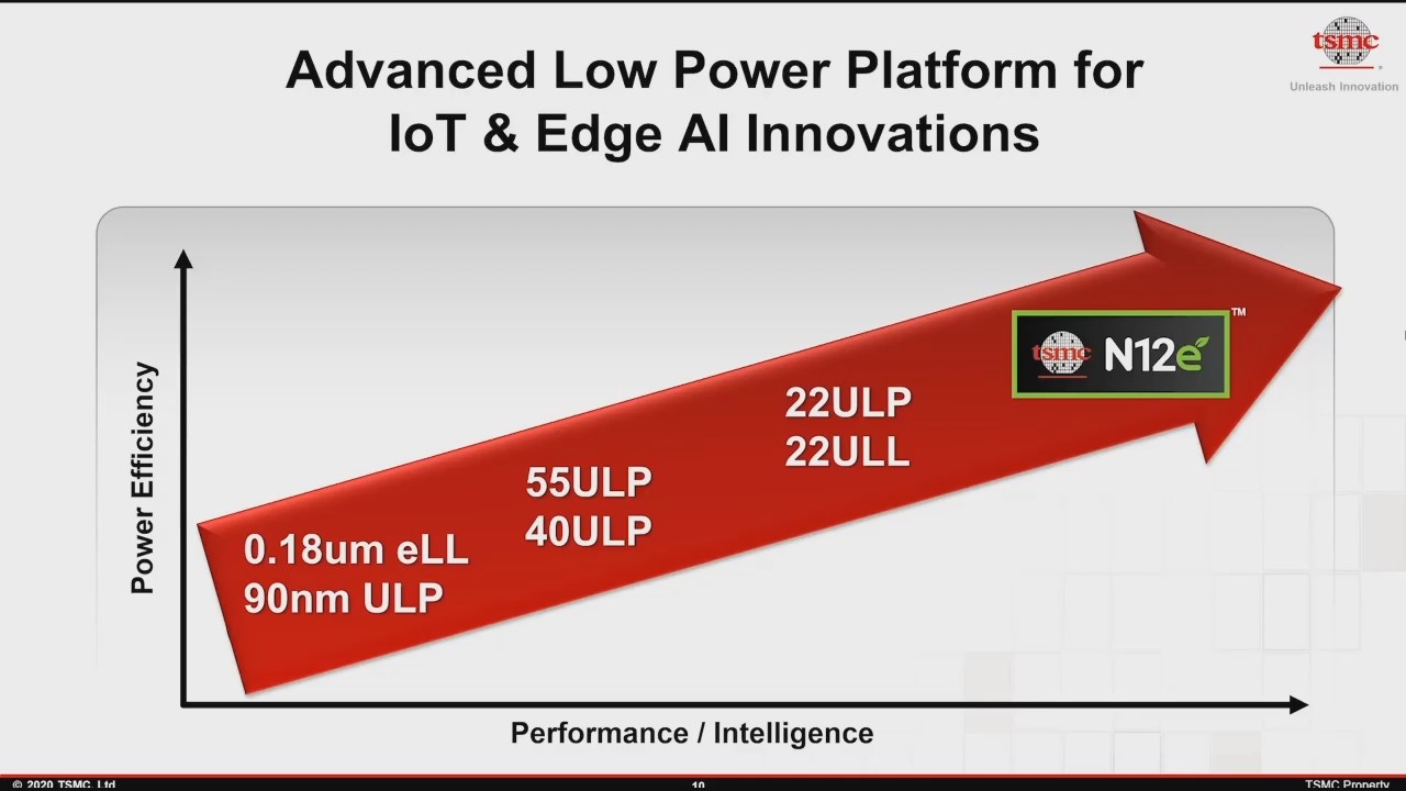
FinFETs are, in a like-for-like situation, extra advanced to construct than planar transistors, and due to this fact ought to naturally value extra to provide. However, FinFET applied sciences additionally present advantages in scaling and energy, one thing this market is keen on. Rather than introduce FinFETs earlier within the cycle, TSMC has waited just a few generations till it may well deploy its most superior FinFET designs to this market, to assist ease the transition with the advantages {that a} most optimized design may convey.
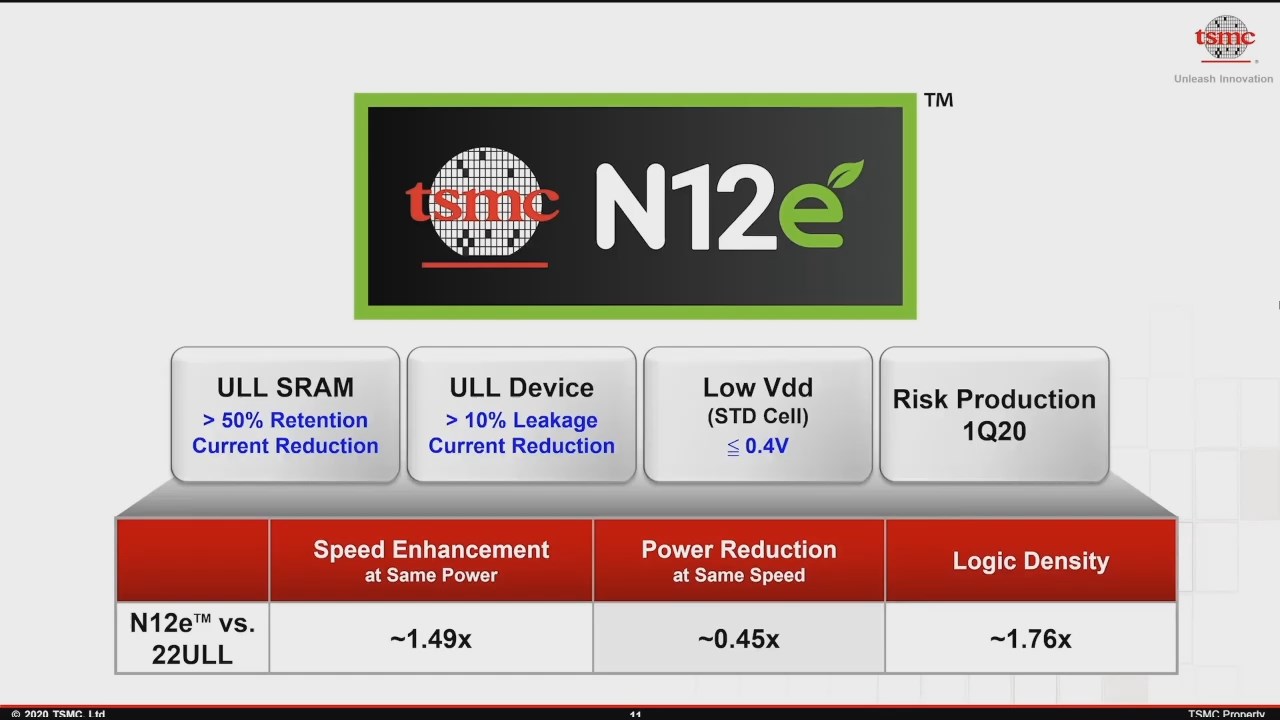
Within N12e in comparison with 22ULL, TSMC is promising a 1.49x enhance in frequency at iso-power, or a 55% discount in energy at iso-speed. This additionally comes with a 1.76x enhance in logic density, and a specialist low-voltage cell library able to 0.four volts. This extends the vary of TSMC’s IoT course of node choices to a decrease energy bracket, in addition to giving a greater efficiency profile in any respect different powers as properly.
N12e brings collectively expertise from TSMC’s 16nm course of and {couples} it with enhancements and expertise from 12FFC+, each of which have been used extensively in excessive efficiency computing. TSMC believes that integrating this with its ultra-low-leakage information will assist allow the following era of 5G-enabled IoT Edge units, by offering low energy routes to AI accelerators for speech recognition, well being monitoring and machine imaginative and prescient.
The essential competitor to N12e can be GlobalFoundries 12FDX platform, which is constructed on GF’s 12nm FD-SOI expertise, with claims of higher energy consumption and decrease value than equal FinFET designs. However regardless of speak of 12 FDX for a number of years (and information of latest MRAM assist and such), there have been no public design wins for the method.
It is unclear when TSMC will begin taking orders for its N12e platform, nonetheless the corporate has mentioned it’s ‘excited’ for the following era of merchandise constructed on it.
Source: TSMC N12e
Related Reading


