
The Snapdragon 820 SoC was a significant milestone on Qualcomm’s roadmap. It was a solid improvement over the 808/810, delivering higher performance and efficiency, and became a commercial success, finding its way into the majority of flagship phones last year. More importantly, it heralded Qualcomm’s vision for mobile devices: heterogeneous computing. This meant new hardware—a much improved Hexagon 680 DSP that added single instruction, multiple data (SIMD) Hexagon Vector Extensions (HVX); Qualcomm’s first fully-custom 64-bit CPU core, Kryo, which focused on improving floating-point IPC; and an updated Adreno GPU with strong ALU performance—for enabling new software technologies and user experiences—artificial intelligence for smarter personal assistants, machine learning for object recognition, computational photography for better image and video quality, and new AR/VR experiences.
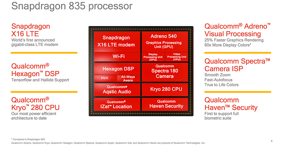
Snapdragon 835—now a part of Qualcomm’s Snapdragon Mobile Platform that includes all of the company’s mobile hardware and software—is an evolutionary product that builds on this vision. The greater than 3 billion transistor SoC is the first to use Samsung’s 10nm “10LPE” FinFET process, which reduces overall package size by 35% relative to Snapdragon 820. The new SoC’s CPU transplant and X16 LTE modem, which tops out at 1Gbps (Category 16) on the downlink, are the biggest changes, but most of the other blocks within the SoC have received at least minor updates too. For detailed information about all the changes and new features, you can read our Snapdragon 835 launch article.
| Qualcomm Snapdragon SoCs: Three Generations | |||
| SoC | Snapdragon 835 (MSM8998) |
Snapdragon 820 / 821 (MSM8996 / MSM8996 Pro) |
Snapdragon 810 (MSM8994) |
| CPU | 4x Kryo 280 Performance @ 2.45GHz 4x Kryo 280 Efficiency @ 1.90GHz |
2x Kryo @ 2.15GHz / 2.34GHz 2x Kryo @ 1.59GHz / 2.19GHz |
4x Cortex-A57 @ 2.00GHz 4x Cortex-A53 @ 1.50GHz |
| GPU | Adreno 540 @ 710MHz ? | Adreno 530 @ 624MHz / 653MHz | Adreno 430 @ 630MHz |
| Memory | 2x 32-bit @ 1866MHz LPDDR4x 29.9GB/s |
2x 32-bit @ 1866MHz LPDDR4 29.9GB/s |
2x 32-bit @ 1600MHz LPDDR4 25.6GB/s |
| ISP/Camera | Dual 14-bit Spectra 180 ISP 1x 32MP or 2x 16MP |
Dual 14-bit Spectra ISP 1x 25MP or 2x 13MP |
Dual 14-bit ISP 1x 21MP |
| Encode/Decode | 2160p30 (2160p60 decode), 1080p120 H.264 & H.265 |
2160p30 (2160p60 decode), 1080p120 H.264 & H.265 |
2160p30 (2160p60 decode), 1080p120 H.264 & H.265 |
| Integrated Modem | Snapdragon X16 LTE (Category 16/13) DL = 1000Mbps 3x20MHz CA, 256-QAM UL = 150Mbps 2x20MHz CA, 64-QAM |
Snapdragon X12 LTE (Category 12/13) DL = 600Mbps 3x20MHz CA, 256-QAM UL = 150Mbps 2x20MHz CA, 64-QAM |
Snapdragon X10 LTE (Category 9) DL = 450Mbps 3x20MHz CA, 64-QAM UL = 50Mbps 1x20MHz CA, 16-QAM |
| Mfc. Process | 10nm LPE | 14nm LPP | 20nm SoC |
In what has become an annual tradition going all the way back to Snapdragon 800, Qualcomm invited the media to its headquarters in San Diego for some feature demonstrations and limited testing using the company’s Mobile Development Platform (MDP) devices. These are fully functional tablets or smartphones in a slightly oversized, utilitarian chassis used for hardware testing and software development. The MDP for Snapdragon 810 took the form of a tablet, while Snapdragon 820 came inside a large smartphone with a 6.2-inch display. This downsizing trend continues for Snapdragon 835, whose MDP/S is a smartphone with 6GB of RAM, a 5.5-inch 2560×1440 display, and a small 2850 mAh battery. The use of a smaller chassis is encouraging, because it has less mass and surface area to absorb and dissipate heat. This suggests a lower TDP for the 835, but we’ll need to measure power consumption to be sure.
Because we only had a limited time for testing, we focused on running some basic CPU, GPU, and memory performance tests. Keep in mind that we were testing prototype hardware running pre-production software that resulted in a few hiccups. The condensed testing period also forced us to stray slightly from our usual testing methodology. Therefore, these numbers should be viewed as preliminary and could change by the time retail units begin shipping.
Snapdragon 820 included Qualcomm’s first fully-custom 64-bit CPU cores. The unique microarchitecture’s floating-point IPC was very good, but integer IPC was no better than ARM’s older A57 core. Its power efficiency was lower than competing cores as well. Instead of using a revised quad-core Kryo arrangement for Snapdragon 835, Qualcomm decided to go in a completely different direction.
The new Kryo 280, despite the similar name, shares no design DNA with the original Kryo. Its an octa-core, big.LITTLE configuration with four “performance” cores and four lower-power “efficiency” cores. What makes Kryo 280 unique, however, is that it’s the first design to use ARM’s new “Built on ARM Cortex Technology” (BoC) license, which allows vendors to customize ARM cores. This new semi-custom option gives vendors the ability to differentiate their products from those using ARM’s stock cores while avoiding the more costly route of creating a fully-custom design from scratch.
The BoC license allows the vendor to request certain modifications, particularly to the fetch block and issue queues, but certain parts of the microarchitecture are off limits, including the decoder and execution pipelines, because modifying these blocks requires too much effort. Qualcomm is not disclosing which ARM cores serve as the foundation for Kryo 280 or precisely which modifications it requested, but it did say that both CPU clusters use semi-custom cores. Qualcomm also confirmed that Snapdragon 835’s memory controllers are its own design.
| Geekbench 4 – Integer Performance Single Threaded |
|||
| Snapdragon 835 | Snapdragon 821 (% Advantage) |
Snapdragon 810 (% Advantage) |
|
| AES | 905.40 MB/s | 559.10 MB/s (61.9%) |
714.47 MB/s (26.7%) |
| LZMA | 3.13 MB/s | 2.20 MB/s (42.3%) |
1.92 MB/s (63.0%) |
| JPEG | 16.80 Mpixels/s | 21.60 Mpixels/s (-22.2%) |
12.27 Mpixels/s (36.9%) |
| Canny | 23.60 Mpixels/s | 30.27 Mpixels/s (-22.0%) |
23.63 Mpixels/s (-0.1%) |
| Lua | 1.84 MB/s | 1.47 MB/s (25.2%) |
1.20 MB/s (53.3%) |
| Dijkstra | 1.73 MTE/s | 1.39 MTE/s (24.5%) |
0.91 MTE/s (90.1%) |
| SQLite | 53.00 Krows/s | 36.67 Krows/s (44.5%) |
33.30 Krows/s (59.2%) |
| HTML5 Parse | 8.67 MB/s | 7.61 MB/s (13.9%) |
6.38 MB/s (35.9%) |
| HTML5 DOM | 2.26 Melems/s | 0.37 Melems/s (510.8%) |
1.26 Melems/s (79.4%) |
| Histogram Equalization | 52.90 Mpixels/s | 51.17 Mpixels/s (3.4%) |
53.60 Mpixels/s (-1.3%) |
| PDF Rendering | 50.90 Mpixels/s | 52.97 Mpixels/s (-3.9%) |
43.70 Mpixels/s (16.5%) |
| LLVM | 196.80 functions/s | 113.53 functions/s (73.3%) |
108.87 functions/s (80.8%) |
| Camera | 5.71 images/s | 7.19 images/s (-20.6%) |
4.69 images/s (21.7%) |
The Snapdragon 835’s Kryo 280 CPU shows a noticeable improvement in integer IPC relative to the 820/821’s Kryo core. This is not unexpected, however, considering integer performance was not one of Kryo’s strengths. While most workloads see large increases, there are a few regressions too, notably in JPEG, Canny, and Camera. We saw this same performance pattern from Kirin 960’s A73 CPU as well. These integer results, along with L1/L2 cache behavior, match the A73’s unique performance fingerprint, confirming that Kryo 280’s performance cores are based on ARM’s latest IP.
Quickly comparing Snapdragon 835 and Kirin 960 Geekbench 4 Integer results also shows performance variations that cannot be fully explained by differences in frequency or normal testing variance. The differences only occur in a few specific tests and range from 9% to -5%, which again is not completely unexpected given the limited number of modifications the BoC license allows for semi-custom designs.
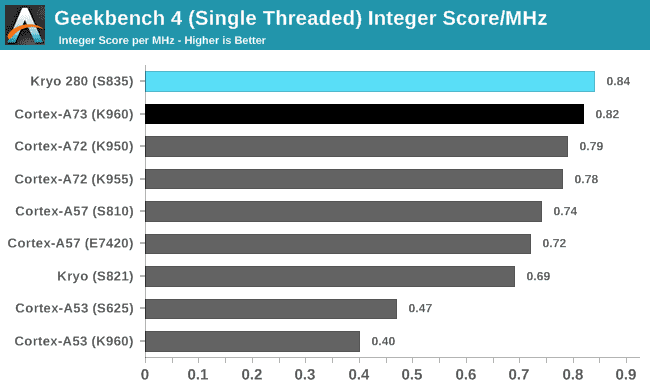
The chart above divides the overall integer score by CPU frequency, making it easier to directly compare IPC. Taken as a whole, the performance of Kryo 280’s semi-custom performance core is not much different than the Kirin 960’s A73 core in this group of workloads, with individual gains and losses nearly averaging out. Its overall IPC is also only about 6% higher than A72 and 14% higher than A57. Its advantage over Snapdragon 820/821 widens to 22%, partly because Kryo’s poor performance in the LLVM and HTML5 DOM workloads drags down its overall score.
While Snapdragon 835 leads other SoCs by a slim margin in this test, it’s not a sweeping victory. Just like we saw with Kirin 960’s A73 cores, performance improves in some workloads but regresses in others.
| Geekbench 4 – Floating Point Performance Single Threaded |
|||
| Snapdragon 835 | Snapdragon 821 (% Advantage) |
Snapdragon 810 (% Advantage) |
|
| SGEMM | 11.5 GFLOPS | 12.2 GFLOPS (-5.7%) |
11.0 GFLOPS (4.2%) |
| SFFT | 2.9 GFLOPS | 3.2 GFLOPS (-9.7%) |
2.3 GFLOPS (25.2%) |
| N-Body Physics | 879.6 Kpairs/s | 1156.7 Kpairs/s (-24.0%) |
580.2 Kpairs/s (51.6%) |
| Rigid Body Physics | 6181.7 FPS | 7171.3 FPS (-13.8%) |
4183.4 FPS (47.8%) |
| Ray Tracing | 232.6 Kpixels/s | 298.7 Kpixels/s (-22.0%) |
130.1 Kpixels/s (78.7%) |
| HDR | 7.8 Mpixels/s | 10.8 Mpixels/s (-27.6%) |
6.4 Mpixels/s (21.9%) |
| Gaussian Blur | 23.4 Mpixels/s | 48.5 Mpixels/s (-51.8%) |
21.9 Mpixels/s (6.7%) |
| Speech Recognition | 13.9 Words/s | 10.9 Words/s (27.5%) |
8.1 Words/s (71.4%) |
| Face Detection | 513.8 Ksubs/s | 685.0 Ksubs/s (-25.0%) |
404.4 Ksubs/s (27.0%) |
Snapdragon 835’s Kryo 280 takes two steps backwards when running Geekbench 4’s floating-point workloads, finishing well behind Snapdragon 820/821’s Kryo core and even a little behind SoCs using the A72 core. Its IPC is on par with the Kirin 960’s A73 core, with even less variation between individual scores than we saw when running the integer…


