
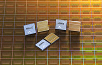
So far, the corporate has managed to fabricate and pattern 512Gb 176-layer 3D NAND chips, so the 600-layer options are nonetheless far-off. Nonetheless, it’s a risk that we’re . Before we attain that layer quantity, there are numerous issues wanted to be solved so the expertise can work. According to SK Hynix, “the company introduced the atomic layer deposition (ALD) technology to further improve the cell property of efficiently storing electric charges and exporting them when needed, while developing technology to maintain uniform electric charges over a certain amount through the innovation of dielectric materials. In addition to this, to solve film stress issues, the mechanical stress levels of films is controlled and the cell oxide-nitride (ON) material is being optimized. To deal with the interference phenomenon between cells and charge loss that occur when more cells are stacked at a limited height, SK Hynix developed the isolated-charge trap nitride (isolated-CTN) structure to enhance reliability.”
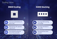
When it involves DRAM, the corporate is trying to overcome some very fascinating issues. By utilizing excessive ultraviolet (EUV) lithography, the corporate can remedy the limitation of patterning on non-EUV processes. Things are wanting very shiny and the method ought to get beneath 10 nm simply. To hold the cell capacitance in test, SK Hynix is making an attempt to refine the dielectric thickness and develop new supplies with excessive dielectric fixed. All of these capacitive cells have to interconnect, and to get as low resistance as potential, the corporate is engaged on the next-generation electrode and insulating supplies.
However, this isn’t all the things that the South Korean firm has to work on. The CEO talked concerning the convergence of reminiscence and logic, with the present business development being simply that. So far, we’ve seen processing close to reminiscence, like we see with chips with HBM stacked simply subsequent to it; processing in reminiscence, the place the processor is current with reminiscence in a single package deal. But, SK Hynix desires to make use of a brand new method of computing in-memory idea, the place the reminiscence is able to performing computation by itself. Applications comparable to AI and machine studying would profit probably the most, together with different makes use of we consider within the meantime. What we’ll find yourself with isn’t recognized, as the corporate solely showcased an idea, so the ultimate merchandise are nonetheless just a few years away.


