
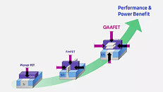
During the IEEE International Solid-State Circuits Conference (ISSCC), Samsung Foundry has offered a brand new step in the direction of smaller and extra environment friendly nodes. The new chip that was offered is a 256 Gb reminiscence chip, primarily based on SRAM know-how. However, all of that does not sound attention-grabbing, till we point out the know-how that’s behind it. Samsung has for the primary time manufactured a chip utilizing the corporate’s gate-all-around field-effect transistor (GAAFET) know-how on the three nm semiconductor node. Formally, there are two varieties of GAAFET know-how: the common GAAFET that makes use of nanowires as fins of the transistor, and MBCFET (multi-bridge channel FET) that makes use of thicker fins that are available in a type of a nanosheet.

Samsung has demonstrated the primary SRAM chip that makes use of MBCFET know-how at present. The chip in query is a 256 Gb chip with an space of 56 mm². The achievement Samsung is happy with is that the chip makes use of 230 mV much less energy for writes, in comparison with the usual method, because the MBCFET transistors enable the corporate to have many various power-saving methods. The new three nm MBCFET course of is anticipated to get into high-volume manufacturing someday in 2022, nonetheless, we’re but to see demos of logic chips in addition to SRAM like we see at present. Nonetheless, even the demonstration of SRAM is huge progress, and we’re desirous to see what the corporate manages to construct with the brand new know-how.


