
Latest QLC V-NAND combines a number of breakthrough applied sciences, together with Channel Hole Etching that permits the very best layer depend within the {industry} with double stack construction
Industry-first QLC and TLC Ninth-gen V-NAND delivers optimum reminiscence throughout varied AI purposes
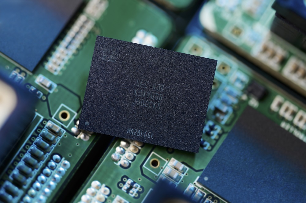
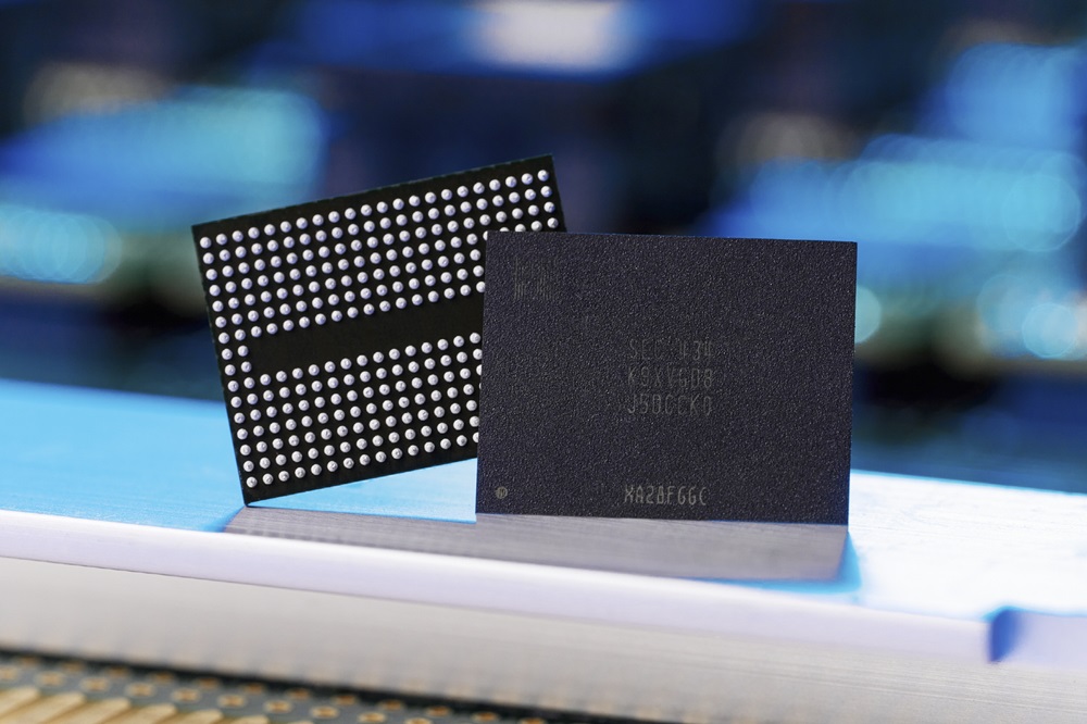
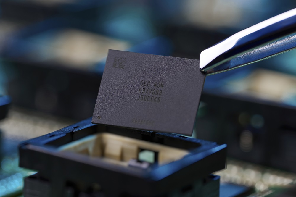
Samsung Electronics, the world chief in superior reminiscence expertise, right now introduced it has begun mass manufacturing of its one-terabit (Tb) quad-level cell (QLC) Ninth-generation vertical NAND (V-NAND).
With the {industry}’s first mass manufacturing of QLC Ninth-generation V-NAND, following the {industry}’s first triple-level cell (TLC) Ninth-generation V-NAND manufacturing in April this 12 months, Samsung is solidifying its management within the high-capacity, high-performance NAND flash market.
“Kicking off the profitable mass manufacturing of QLC Ninth-generation V-NAND simply 4 months after the TLC model permits us to supply a full lineup of superior SSD options that handle the wants for the AI period,” mentioned SungHoi Hur, Executive Vice President and Head of Flash Product & Technology at Samsung Electronics. “As the enterprise SSD market shows rapid growth with stronger demand for AI applications, we will continue to solidify our leadership in the segment through our QLC and TLC 9th-generation V-NAND.”
Samsung plans to broaden purposes of the QLC Ninth-generation V-NAND, beginning with branded client merchandise and lengthening into cell Universal Flash Storage (UFS), PCs and server SSDs for patrons together with cloud service suppliers.
Samsung’s QLC Ninth-generation V-NAND brings collectively a variety of improvements that have produced technological breakthroughs:
- Samsung’s unequalled Channel Hole Etching expertise was used to attain the very best layer depend within the {industry} with a double stack construction. Utilizing the technological experience gained from the TLC Ninth-generation V-NAND, the world of the cells and the peripheral circuits have been optimized, reaching an industry-leading bit density roughly 86% larger than that of the earlier era QLC V-NAND.
- Designed Mold expertise adjusts the spacing of Word Lines (WL), which function the cells, to make sure uniformity and optimization of cell traits throughout and inside layers. These traits have develop into more and more vital because the V-NAND layer counts enhance. Adopting Designed Mold has improved knowledge retention efficiency by roughly 20% in comparison with earlier variations, resulting in enhanced product reliability
- Predictive Program expertise anticipates and controls cell state adjustments to attenuate pointless actions. Samsung’s QLC Ninth-generation V-NAND has doubled write efficiency and improved knowledge enter/output pace by 60% via developments to this expertise.
- Data learn and write energy consumption decreased by about 30% and 50% respectively, with using Low-Power Design This technique reduces the voltage that drives NAND cells and minimizes energy consumption by sensing solely the mandatory bit traces (BL).


