
Yesterday, Samsung Electronics had introduced a brand new 3D IC packaging know-how known as eXtended-Cube, or “X-Cube”, permitting chip-stacking of SRAM dies on high of a base logic die by means of TSVs.
Current TSV deployments within the trade largely come within the type of stacking reminiscence dies on high of a reminiscence controller die in high-bandwidth-memory (HBM) modules which are then built-in with extra complicated packaging applied sciences, reminiscent of silicon interposers, which we see in at the moment’s high-end GPUs and FPGAs, or by means of different complicated packaging reminiscent of Intel’s EMIB.
Samsung’s X-Cube is kind of totally different to those present applied sciences in that it does away with middleman interposers or silicon bridges, and straight connects a stacked chip on high of the first logic die of a design.
Samsung has constructed a 7nm EUV take a look at chip utilizing this system by integrating an SRAM die on high of a logic die. The logic die is designed with TSV pillars which then hook up with µ-bumps with solely 30µm pitch, permitting the SRAM-die to be straight related to the principle die with out middleman mediums. The firm that is the trade’s first design such design with a sophisticated course of node know-how.
It’s not the primary time that the corporate has demonstrated TSVs within the base logic die to hook up with a stacked die on high of it. Back in 2013, the corporate had confirmed customized Exynos chips utilizing Widcon know-how, stacking Wide I/O DRAM reminiscence on high of the bottom logic chip with assist of TSVs, providing a higher-performance and decrease energy answer in comparison with conventional PoP reminiscence. Unfortunately, this know-how by no means noticed the sunshine of day in client units because it doubtless by no means was cost-effective sufficient justify for mass-production.
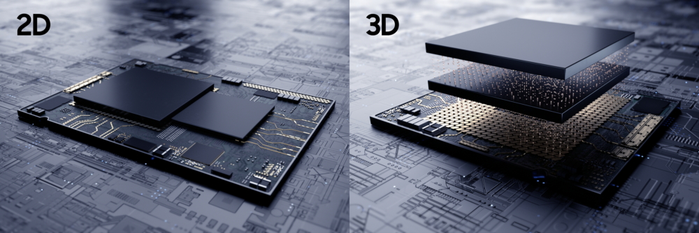
Stacking extra beneficial SRAM as a substitute of DRAM on high of the logic chip would doubtless symbolize the next worth proposition and return-on-investment to chip designers, as this might permit smaller die footprints for the bottom logic dies, with bigger SRAM cache buildings with the ability to reside on the stacked die. Such a big SRAM die would naturally additionally permit for considerably extra SRAM that will permit for larger efficiency and decrease energy utilization for a chip.
Samsung’s advertising and marketing supplies showcase greater than a single die of SRAM, which might point out that X-Cube may be variable by way of its stack-height. It’s at the moment unclear if X-Cube can be restricted to SRAM dies, or whether or not it would additionally lengthen to future logic-over-logic stacking.
Samsung is offering silicon confirmed design methodology and circulation for its superior 7nm and 5nm nodes, and states that X-Cube can be utilised for superior functions reminiscent of cellular, AR/VR, wearable and HPC designs. The firm can also be planning a presentation on X-Cube at Hot Chips this Sunday the place it would revealing extra particulars on the know-how.


