
This results in numerous difficulties for events to really glean any significant data from this specific semiconductor metric alone. Now, a staff of researchers has tackled this drawback by suggesting a distinct method to specific semiconductor manufacturing functionality. Their intention is to permit to “gauge advances in future generations of semiconductor technologies in a holistic way, by accounting for the progress in logic, memory, and packaging/integration technologies simultaneously.” As such, their proposed density metric follows a [DL, DM, DC] philosophy, the place DL is the density of logic transistors (in #/mm²), DM is the bit density of most important reminiscence (at the moment the off-chip DRAM density, in #/mm²), and DC is the density of connections between the primary reminiscence and logic (in #/mm²). The researchers say that present high semiconductor expertise density out there can be described by this method as [38M, 383M, 12K].
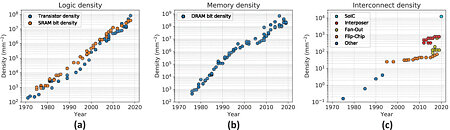
The researchers embody metrics comparable to DM and DC as a result of present pc programs completely rely on off-chip reminiscence density, and I/O and precise logic/reminiscence throughput is more and more necessary in all computing situations (and particularly as computing efficiency will increase). Furthermore, the researchers have famous a comparable improve in density of logic transistors and DRAM bit density, which provides to this new density metric. Remember that these values are speculated to signify the utmost efficient functionality of any given manufacturing course of – because of this a next-generation course of from Intel may embody most transistor density expressed in the results of an equation so simple as variety of transistors divided by the die space; the utmost out there DRAM bit density of reminiscence that may be paired with this fabrication course of chip (we count on this quantity to be modified throughout product portfolios in a given era ought to appropriate DRAM density developments happen within the lifetime of a given die logic manufacturing lifetime; in addition to density of logic-to-memory connectivity.
Considering the present naming conference panorama for manufacturing course of density is… stuffed with as many plot-holes as some super-hero franchises, this looks as if a wise method to go about in truly forcing a degree enjoying subject between producers. They hold their leeway in advertising phrases to explain their processes as they need, however should additionally present these density metrics for his or her course of applied sciences. And since this refers back to the most densities their course of can help (relating to transistor logic and reminiscence connection logic densities), it ensures that customers, establishments, and firms can truly take a look at the semiconductor panorama with a transparent image.


