The new version of the throughput technology will provide a massive bandwidth improvement to GPUs next year

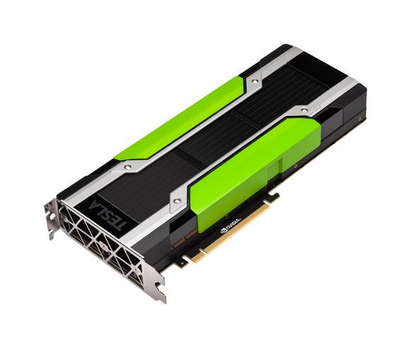
Nvidia’s Tesla P100 plugs into a PCI-Express 3.0 slot.
Graphics processors with Nvidia’s NVLink throughput technology have just started coming out, but a successor to the groundbreaking interconnect is already on its way.
IBM’s upcoming Power9 chip will include NVLink 2.0 technology, and servers using the chip will be available next year.
Nvidia hasn’t yet announced when GPUs with NVLink 2.0 would come out, but they could be available around the same time as the new Power9 servers come out.
IBM is projecting Power9 servers to be out by the middle of next year, but the company hasn’t nailed down a specific date.
A presentation on Nvidia’s website says NVLink 2.0 will be in GPUs code-named Volta, which also will come out next year.
Each NVLink 2.0 lane in the Power9 chip will communicate at 25Gbps (bits per second), seven to 10 times the speed of PCI-Express 3.0, according to IBM. Power9 will have multiple communication lanes for NVLink 2.0, and they could provide massive throughput when combined.
Recent Nvidia GPUs like the Tesla P100 are based on the company’s Pascal architecture and use NVLink 1.0. The Volta GPU architecture will succeed Pascal, also used in GPUs like the GeForce GTX 1080.
With a tremendous bandwidth improvement in over its predecessor, the NVLink 2.0 technology will be important for applications driven by GPUs, like cognitive computing.
Nvidia is a key member of OpenPower Foundation, an IBM-backed organization that is trying to proliferate Power hardware and software.
For now, the NVLink 2.0 I/O is designed for Nvidia GPUs, and no other component works with the interconnect. IBM’s Power chip also offers the PCI-Express 4.0 connector and a CAPI (coherent accelerator processor interface) interface for other chips, storage, and memory.


![[World Sleep Day] How Samsung Is Tackling Sleep Apnea to](https://loginby.com/itnews/wp-content/uploads/2026/03/1773427850_World-Sleep-Day-How-Samsung-Is-Tackling-Sleep-Apnea-to-100x75.jpg)
