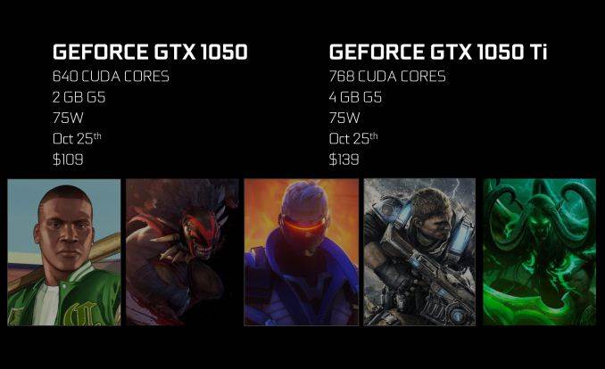
After a break of a couple of months in their Pascal launch schedule, NVIDIA is back again to launch a new Pascal desktop product. Following their near-perfect top-down launch schedule that started with GeForce GTX 1080 in May, being announced today and formally launching next week is the GeForce GTX 1050 Ti and GeForce GTX 1050. Aimed at the entry level discrete video card market, these products will round-out the GeForce 10-series desktop lineup.
Launching their low-tier cards last instead of first for the Pascal generation marks an interesting inverse of what happened with the Maxwell generation. In 2014 it was the low-end Maxwell 1 parts that launched first, only to be followed up by the other Maxwell 2 parts later on in the year. As a result, the Maxwell 2 family went through a full cycle – from release to retirement – before NVIDIA’s entry-level cards were refreshed. Out of all of the segments in the NVIDIA product stack, it’s fair to say that the entry-level was the one most due for a refresh.
And to that end, here we are with the GeForce GTX 1050 series. The previous GeForce GTX 750 series went very well for NVIDIA, so much so that the new 1050 series follows a number of beats laid out by its predecessor. NVIDIA is launching two cards – both of which are based on the new GP107 – which setup a two-tier product offering for the entry level market. The fast of the two cards is the GTX 1050 Ti, while the GTX 1050 follows closely to offer a bit less performance at a lower price point. And in order to maximize compatibility, both cards are being offered in configurations that draw their power entirely from the PCIe bus, forgoing the need for an external power connection.
| NVIDIA GPU Specification Comparison | |||||||
| GTX 1060 3GB | GTX 1050 Ti | GTX 1050 | GTX 750 Ti | GTX 750 | |||
| CUDA Cores | 1152 | 768 | 640 | 640 | 512 | ||
| Texture Units | 72 | 48 | 40 | 40 | 32 | ||
| ROPs | 48 | 32 | 32 | 16 | 16 | ||
| Core Clock | 1506MHz | 1290MHz | 1354MHz | 1020MHz | 1020MHz | ||
| Boost Clock | 1709MHz | 1392MHz | 1455MHz | 1085MHz | 1085MHz | ||
| Memory Clock | 8Gbps GDDR5 | 7Gbps GDDR5 | 7Gbps GDDR5 | 5.4Gbps GDDR5 | 5Gbps GDDR5 | ||
| Memory Bus Width | 192-bit | 128-bit | 128-bit | 128-bit | 128-bit | ||
| VRAM | 3GB | 4GB | 2GB | 2GB | 1GB | ||
| FP64 | 1/32 | 1/32 | 1/32 | 1/32 | 1/32 | ||
| TDP | 120W | 75W | 75W | 60W | 55W | ||
| GPU | GP106 | GP107 | GP107 | GM107 | GM107 | ||
| Transistor Count | 4.4B | 3.3B | 3.3B | 1.87B | 1.87B | ||
| Manufacturing Process | TSMC 16nm | Samsung 14nm | Samsung 14nm | TSMC 28nm | TSMC 28nm | ||
| Launch Date | 08/18/2016 | 10/25/2016 | 10/25/2016 | 02/18/2014 | 02/18/2014 | ||
| Launch Price | $199 | $139 | $109 | $149 | $119 | ||
Diving into the specs, we’ll start with the GTX 1050 Ti. Based on a fully enabled GP107 GPU, this card is arguably the backbone of NVIDIA’s entry-level offerings. All-told, it has 6 SMs enabled – 60% that of GP106/GTX 1060 – so GP107 is a bit more than half of a GP106. The rest of the Pascal architecture has been scaled similarly; GP107/GTX 1050 Ti retains 2/3rds of the ROP and memory controller configuration, meaning we’re looking at 32 ROPs attached to a 128-bit memory bus. Notably, this is double the number of ROPs found on GTX 750, so all other factors held equal, GTX 1050 Ti will see a massive jump in ROP throughput compared to its predecessor.
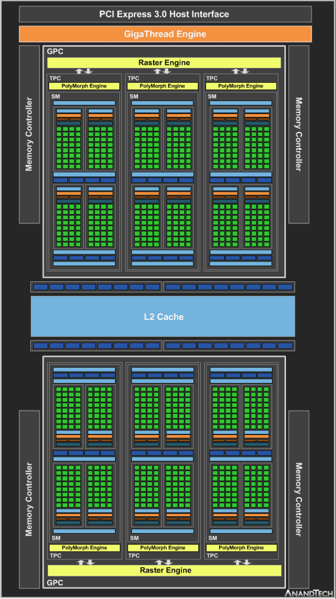
Unofficial GP107 Block Diagram
Feeding GTX 1050 Ti is 4GB of GDDR5 memory, clocked at 7Gbps. This is a budget card – and a power limited one at that – so NVIDIA has pulled back on the memory clocks compared to the other Pascal cards. Meanwhile power consumption starts at 75W, the maximum amount allowed to be pulled from a PCIe slot. I say “starts” because NVIDIA will be allowing partners to sell factory overclocked cards, and these cards will feature a higher TDP and an external power connector in order to meet the card’s power needs. The significance of offering a 75W-and-under card cannot be overstated; there is a sizable market for end users who would like to upgrade an OEM system but don’t have an external power connector, and this is a role the preceding GTX 750 filled very well. Meanwhile HTPC users who were holding out for a 75W card will be equally pleased, as now Pascal’s suite of media features are on a lower power card.
Joining the GeForce GTX 1050 Ti is its smaller, cheaper sibling, the GTX 1050. Based on a cut-down GP107 GPU, GTX 1050 drops 1 SM and 2GB of memory. This leaves us with a 5 SM (640 CUDA core) card paired with 2GB of GDDR5 running at 7Gbps. Otherwise it has the full ROP complement and memory bus, so while GTX 1050 loses some shader and geometry throughput, in other areas it holds firm. In fact due to the unusual clockspeeds of these cards – more on this in a moment – the GTX 1050 is actually clocked higher than the GTX 1050 Ti. So the net performance difference on paper is less than the loss of the SM; the smaller card should offer around 87% of the GTX 1050 Ti’s performance. With that said, unlike the last generation you don’t save any power versus the Ti card when going by the official TDP, as the GTX 1050 is also a 75W card, which happens to be 20W more than the GTX 750. Consequently while it’s still a card that can run on just PCIe slot power, by NVIDIA’s own numbers we may be looking at a relatively sizable increase in power consumption relative to its predecessor.
GP107 – An Enigma of a GPU
Having covered the basic specifications, I want to spill a bit more ink talking about the GP107 GPU. Reading the specs table, the GTX 1050 series cards are very unusual compared to their more powerful siblings. To be sure they’re still Pascal cards, but certain elements we take for granted about the Pascal family don’t apply here. At the same time there are certain elements we take for granted about x50 series cards which also aren’t applicable here. GP107 is, at the moment, an enigma of a GPU.
I’ll address what’s likely the elephant in the room first, which is the manufacturing process. To date all Pascal GPUs have been fabbed over at TSMC on their 16nm FinFET process. GP107 is not one of those GPUs. Instead, it’s fabbed on a 14nm process – NVIDIA’s specification sheet doesn’t technically state whose process – but by simple elimination it’s a very safe bet that they’re making the chip over at Samsung. Feature size is a red herring here, and instead the significance of this deal is that NVIDIA has not used a fab other than TSMC for GPUs for a long time. In fact we’d have to go back to 2003 to find an NVIDIA GPU fabbed somewhere else, when NVIDIA tapped IBM to help fab the ill-fated NV3x series (GeForce FX).
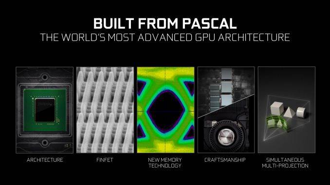
Suffice it to say, tapping another fab is a very big deal. There’s no second-sourcing here – GP107 is only being made on Samsung’s 14nm process and GP106+ only on TSMC’s 16nm process – but splitting orders like this may just as well be new territory for NVIDIA. As this is just a product announcement NVIDIA hasn’t said anything about the change in fabs, so let your imagination go wild here, but it definitely has some ramifications. I really need to get the GTX 1050 cards in house and on the testbed to figure out the full ramifications of this, but I think the most important change here is that a new process from a new vendor means that the voltage/frequency curve we’ve come to know with TSMC 16nm and Pascal has essentially been thrown out the window.
This in turn may explain the clockspeeds of the GTX 1050 cards. All of the other desktop GeForce 10-series cards have an official boost clock of 1600MHz+, with all but one of those cards being 1700Mhz+. The massive jump in clockspeed relative to Maxwell 2 is one of the signature elements of the Pascal architecture, and a major factor driving the significant performance gains of this generation compared to the last. The GTX 1050 series, by comparison, is only rated to boost up to 1455MHz for the GTX 1050, and lower still for the GTX 1050 Ti at 1392MHz.
Given that these are power-constrained cards, the final specifications of the cards are bound by a larger number of variables than usual – power curves, attainable frequency range, and now total power consumption – so I’m not even going to try to insinuate that the lower clockspeeds are solely a function of the change in fabs. However it’s very important to keep in mind that these lower clockspeeds come with a sometimes sizable increase in TDP relative to the GTX 750 series; instead of 55W/60W cards, we have 75W cards. So to use the fully enabled GTX 1050 Ti as an anchor point, power consumption has gone up 15W (25%) for a 28% increase in the boost clock, 1 more SM (20%), and somewhat decoupled from this, the doubled ROP count.
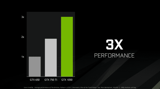
It’s telling then that NVIDIA has informed the press that the higher TDP cards with an external power connector are going to have much higher boost clocks. Whatever is going on under the hood, power plays a big part, and at a TDP limit of 75W, GP107 isn’t getting all the room it needs to stretch. Meanwhile it’s also noteworthy that NVIDIA’s own marketing materials call for GTX 1050 to have a 3x performance increase over GTX 650, and only a bit over 50% increase over GTX 750 Ti.
At the same time though, keep in mind we’re looking at a generation and a half architectural jump from the GTX 750 series (GM107) to the GTX 1050 series (GP107). So NVIDIA has to spend quite a bit of their transistor budget on supporting new features, and not just graphical features like SMP and Feature Level 12_1, but also features like the new video display block and the full fixed-function HEVC encode and decode blocks. By virtue of being the smallest Pascal, GP107 spends relatively more die size and space on non-graphics…
