
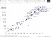
For a interval longer than 5 a long time the rule of Moore’s Law has labored, making the above graph look virtually linear if a line could be drawn. What attracts the road away from its linearity are occasional hiccups in manufacturing that the business needed to take care of and did overcome ultimately. Through historical past, Moore’s Law has been declared and predicted to be lifeless many occasions, because the business approached sub-micron sizes. Starting from 1 µm, many individuals grew to become skeptical within the regulation’s viability and the way effectively wouldn’t it maintain up, however time has proved these individuals improper and we at the moment are already utilizing merchandise which can be based mostly on 7 nm node.
The problem
What actually is attempting to cease the regulation are three issues: lithography, impurities and economies of scale.
First downside to handle are impurities discovered on the atom degree. Silicon manufacturing foundries are melting quartz sand to kind a giant crystal construction that’s lower up into wafers. When sand is melted, impurities are inevitable. That is because of the truth that heating silicon makes it simply react with the halogens (fluorine, chlorine, bromine, and iodine) to kind halides. Those halides are eliminated through the use of extra chemical substances that dissolve and take away them so a giant crystal may be extracted for making of wafers. “What’s the problem caused by removal of these impurities?”, you would possibly ask. The smaller the scale of a person transistor, likelihood is higher that even a small atom of impurities, left over from earlier cleansing, might be current and render a transistor unusable.
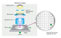
The second downside to handle is lithography. In order to make the transistors, you must “print” them on a silicon wafer. That is finished by shining gentle via a mildew referred to as masks, which penetrates the silicon and etches the sample right into a wafer. Naturally, as you lower the scale of your transistor, you must make your masks smaller. The smaller the masks, the tougher it’s to make it (you begin to discover a sure sample right here with measurement decreases). So to resolve this downside, the semiconductor business has made a multi-patterning method which takes a number of turns into the etching course of to be able to enhance the effectivity of the masks utility. However, typically occasions this method will not be sufficient and UV gentle is having hassle printing designs to silicon. That’s how Extreme UV or EUV lithography was born. It makes use of a stronger gentle supply with a shorter wavelength to raised etch the design and thus cut back the errors the printing would possibly encounter. What the issue actually is right here, will not be the sunshine that passes via the masks, it’s the masks itself. The masks is the essential design component because it transfers your design to silicon. If you can’t make exact and small masks, you can’t get a working chip. Thus, the making of the masks is one other essential step that makes Moore’s regulation exhausting.
The third and remaining downside is economics of scale. That is the place the much less identified Moore’s second regulation is available in, which predicts that the price of organising a brand new manufacturing facility can also be getting two occasions dearer each two years. Today to be able to construct a brand new fab, firms are spending billions of {dollars}. Intel has invested greater than $12B in its fab quantity 42 in Arizona, imagined to manufacture 7 nm chips some day. In addition to the massive capital wanted to simply open a brand new fab, firms must develop its personal semiconductor node course of. To put issues into perspective, business speculations are that ranging from 5 nm…


