
The programmability of a processor is a scale is all about flexibility and efficiency – one thing extremely programmable and customizable is adaptable to all type of conditions, however typically isn’t as quick. However, one thing that has a really specified compute pathway can go very quick, however can’t do a lot past that pathway. On the versatile facet, we now have FPGAs, that may be configured to do virtually something. On the fastened facet, we now have ASICs, corresponding to fastened operate {hardware} for AI. Somewhere within the center is what’s referred to as a ‘Structured ASIC’, which tries to mix as many advantages from the 2.
An FPGA, or Field Programmable Gate Array, is a bit of silicon constructed that may be configured after manufacturing. By implementing a sequence of programmable logic blocks, reminiscence cells, and layers of connectivity, a programmer with sufficient data can configure the FPGA to run the equal of distinctive circuit designs for particular features. For instance, any sequence of AI calculations could be finished on a CPU core slowly, and a subset of them could be very quick on a GPU, but when that calculation methodology has to alter, the FPGA could be adjusted to be GPU-like of effectivity whereas being as configurable because the CPU.
An ASIC, in contrast, is a really fastened unit of {hardware}. By understanding what kind of calculations are anticipated, an ASIC can implement these calculations very quick and really effectively, however it may possibly solely do this type of calculation. For instance, a graphics card could be considered an ASIC, because it does graphics very nicely, nonetheless the particular 4K decode engine contained in the GPU is best suited to the time period of an ASIC, as a result of all it does is decode 4K pictures/video and it is aware of learn how to do it a lot sooner and rather more effectively than a CPU or an FPGA might.
Obviously if there are safety considerations, an FPGA has the flexibility to maybe be configured to keep away from that problem. An ASIC in contrast has no resolution. FPGAs could be deployed with updates to be despatched later, whereas ASICs can’t be up to date. FPGAs are initially very low-cost, and ASICs require a whole lot of up-front non-reusable engineering (NRE) prices, nonetheless when constructed at scale, can provide one thing cheaper at orders of magnitude decrease energy and better efficiency. These are among the trade-offs.
A structured ASIC (or for Intel, an eASIC), is one thing between the 2. The underlying design of an eASIC product is much like an FPGA, however by doing a little small upfront NRE/circuit design, an eASIC firm modifications a few of its silicon manufacturing masks for FPGAs for the design in query. This implies that the eASIC is not as configurable as an FPGA because it now has some inflexible pathways in its silicon, but it surely takes positive aspects among the efficiency and energy effectivity by having inflexible pathways. It additionally hasn’t required the massive quantity of design prices {that a} full ASIC requires, and thus saves a whole lot of price, and the product finally ends up someplace between an FPGA and an ASIC.
For any firm focused on one thing like a structured ASIC, it means creating a relationship with a vendor providing a portfolio of structured ASIC base designs, after which implementing some stage of circuit customization on high on the level of manufacture.
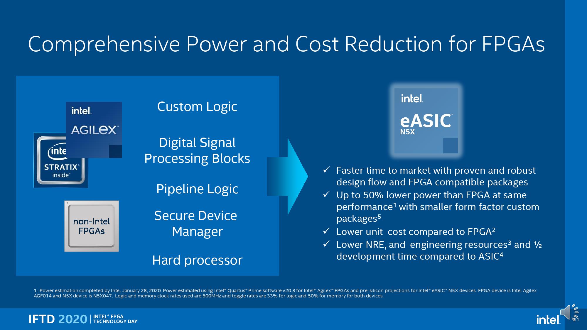
Intel not too long ago bought an organization referred to as eASIC in mid-2018 to do exactly this, and the primary line of merchandise are referred to as the N5X eASICs (Diamond Mesa, for anybody following code names), which add-in hardened embedded CPU cores to permit for management and safety. A variety of applied sciences have been pulled in from the Intel Agilex FPGA household to enhance the earlier eASIC providing, in addition to a software program platform.
The N5X sequence base design is constructed on a 16nm course of (TSMC, by advantage of the acquisition), makes use of as much as 80 million eASIC gates (8.Eight million FPGA-like search for…


