
One of the problems going through next-generation 3D stacking of chips is improve the density of the die-to-die interface. More connections means higher knowledge throughput, decreasing latency and rising bandwidth between two energetic areas of silicon that could be manufactured at completely different course of nodes. There’s additionally a consideration for energy and thermal hotspots as properly. Intel has been creating its personal bodily interconnect topologies, most of which we’ve lined intimately earlier than, such because the Embedded Multi-Die Interconnect Bridge (EMIB) that enables 2D growth and Foveros die-to-die 3D staking that permits vertical growth. As a part of Intel’s Architecture Day 2020, now we have a glimpse into Intel’s future with hybrid bonding.
There are a number of holistic metrics to measure how ‘good’ an interconnect could be; the 2 which are best to grasp are density of connections (bump density) and power (how a lot power it takes to switch a bit).
Intel’s Ramune Nagisetty showcasing present packaging applied sciences at Intel
Intel’s personal slides present us that EMIB’s bump density is sweet for ~400 per sq. millimeter, with an influence of 0.50 petajoules per bit transferred. Foveros takes {that a} step additional, supporting 400-1600 bumps per sq. millimeter, and a median energy of 0.15 petajoules per bit transferred.
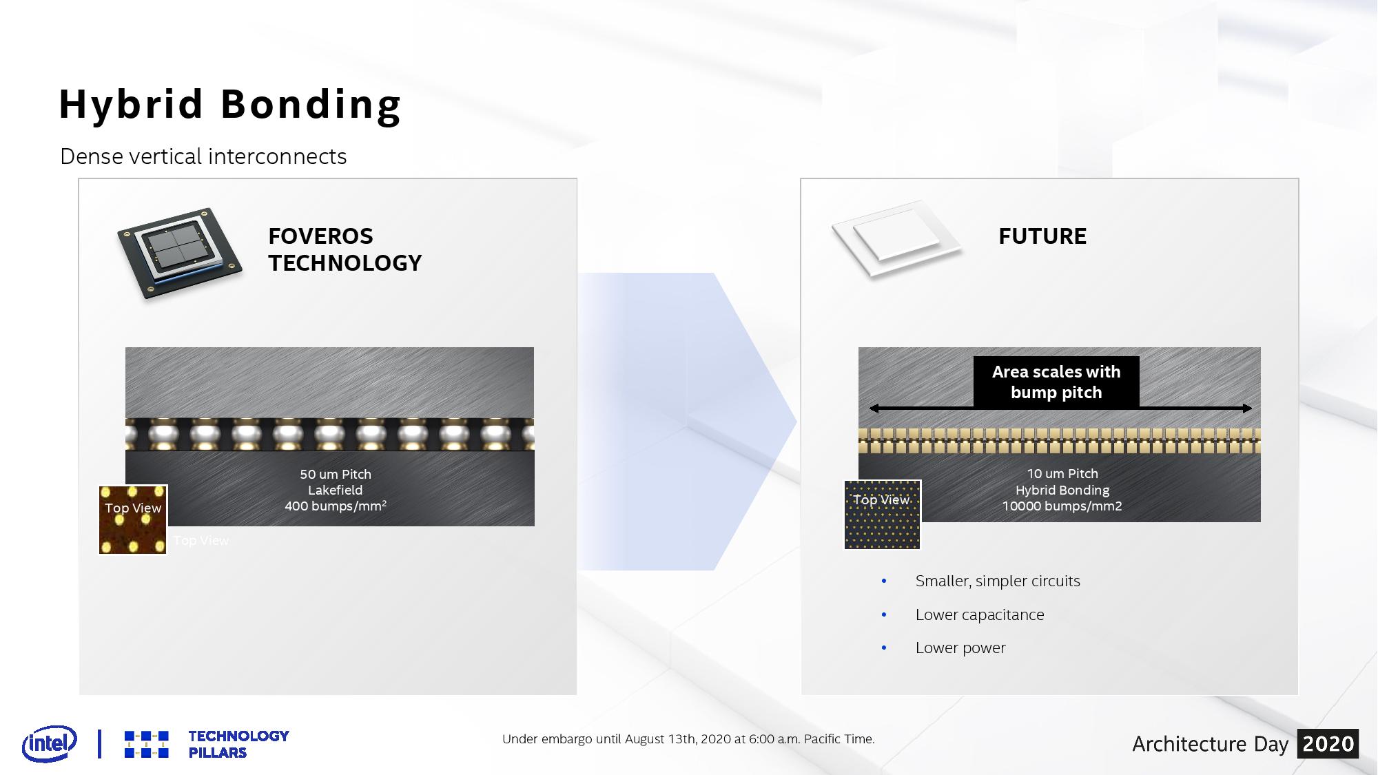
The subsequent period of ‘Hybrid Bonding’ that Intel goes in the direction of improves each metrics by round an element of 3-10. The new take a look at chips that Intel has simply received again into the lab, involving stacked SRAM, goes in the direction of the 10000 bumps per sq. millimeter vary, with an influence below 0.05 petajoules per bit. According to Intel this enables for smaller and less complicated circuits, with decrease capacitance and higher effectivity. Nothing to be stated about yields nevertheless!
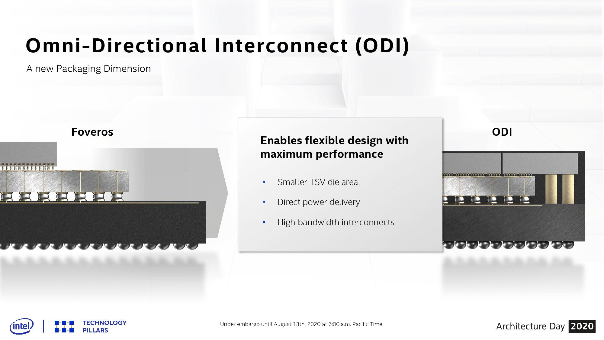
With these new bonding and stacking applied sciences, the query at all times turns into considered one of thermals, and the way Intel would possibly stack two performance-related bits of silicon collectively. In the discussions as a part of Architecture Day, Intel said that these stacked designs require having all layers designed collectively, relatively than independently, with a view to handle {the electrical} and thermal traits. As far as Intel sees it, probably the most energy hungry layer is required to go on the highest of the stack in the meanwhile, which clearly implies that the ability connections need to both stand up by the decrease layers, or there needs to be some type of cantilevered scenario the place energy connections can occur off the sting of the bonding – Intel calls this expertise ODI, to assist completely different sized silicon layers.
With the way forward for excessive efficiency and excessive effectivity computing coming to a head with new packaging applied sciences, discovering the appropriate method of going ahead is ever vital. For a context on timeline, Intel’s Ramune Nagisetty has said that Foveros was patented again in 2008, however it took practically a decade for the method to turn out to be bodily viable at scale and high-enough yielding for a product to return to market.


