
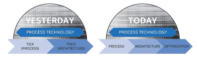
When Intel first announced the shift from the dual-stage ‘Tick-Tock’ methodology that had driven their core CPU design teams for over a decade into the three-way ‘Process, Architecture, Optimization’ paradigm, there were questions as to how much of the final stage, the Optimization, would actually change the way CPUs were presented or offer upgrades in performance. At the time, ‘Kaby Lake’ as the name for Intel’s third crack at their 14nm process was well known, but users wondered if it was just another Devil’s Canyon (better overclocking) or a full on CPU launch. Well the answer is the latter, and the launch is staggered between today and January. Roll on Kaby Lake. Is that Kah-bee Lake, or Kay-bee Lake?
Tick-Tock to Process-Architecture-Optimization (PAO)
Intel’s two year processor cadence of Tick-Tock allowed the company to alternate reducing the lithography node (a tick) with an upgraded microarchitecture (a tock) with modest gains of performance. Each stage of the Tick-Tock would take 12-15 months, with new lithography nodes taking longer and longer to reach maturity. Eventually it has gotten to a point where 14nm took too long to become pervasive in Intel’s product stack. For a manufacturing company and a CPU company, slowly rolling out Broadwell notebook and low power parts and then gutting the mid-range desktop was the result of the troubles of bringing 14nm to the prime time. Now in 2016 we have the launch of full-sized Broadwell-EP server parts running up to 22 cores in a 145W envelope, but the low power parts are a couple of microarchitectures ahead. We have this strange situation of a stretched landscape, partially driven by markets but also for manufacturing.
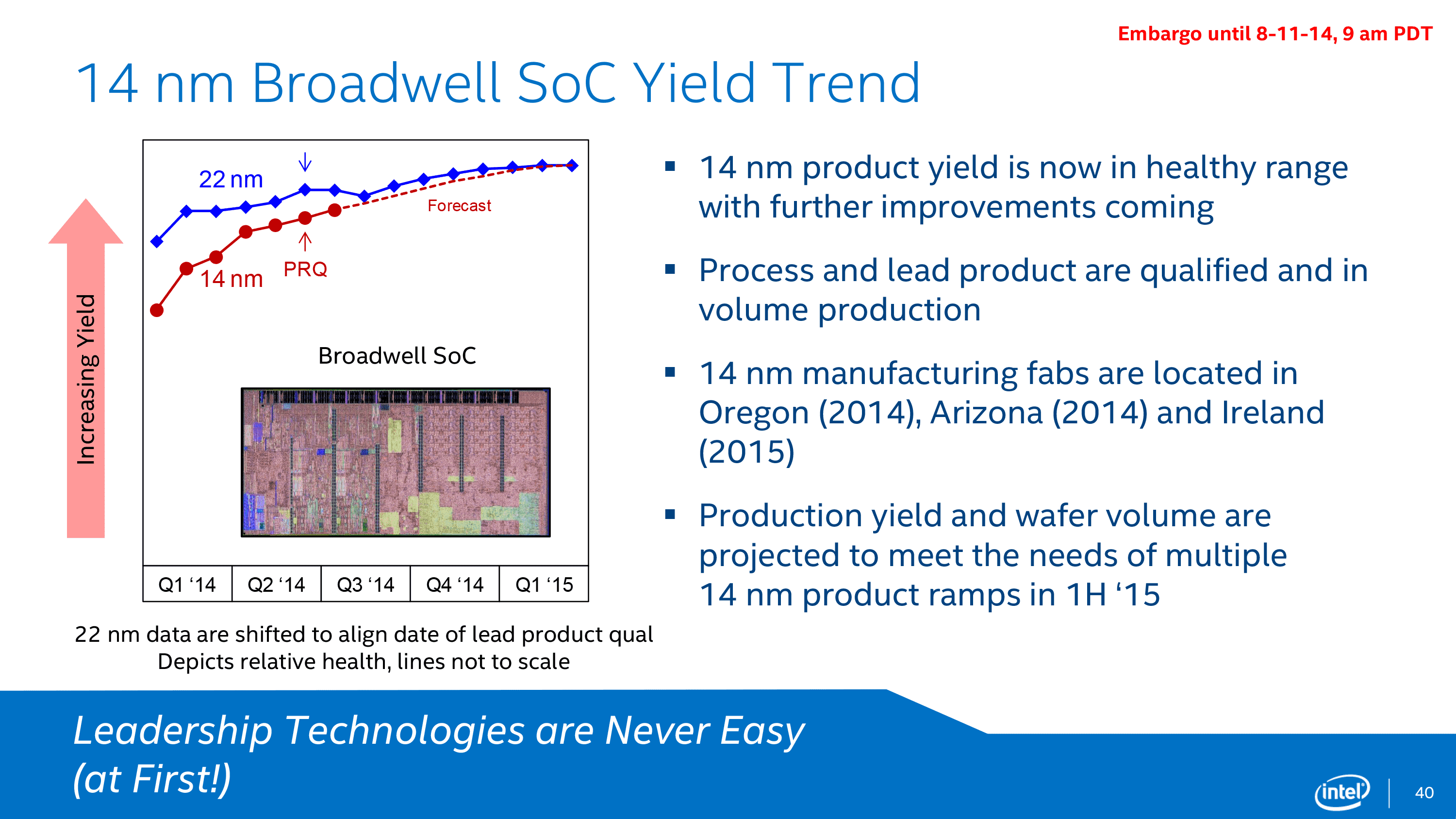
The move from Intel’s 14nm process to 10nm is a long, slow burn, taking much longer to develop than any process previous. We first saw 14nm in Broadwell mobile CPUs in Q3 of 2014, almost two years ago, and 10nm still isn’t on any public roadmap for early 2017. With the tick-tock strategy, and the launch of Skylake in mid-2015, this would leave Intel without a new CPU launch for almost two years, which is unheard of from Intel. Also, Intel’s partners rely on product cycles to announce and launch new products to generate revenue. To fill the gap, plus with a few other techniques, Intel moved to Process-Architecture-Optimization, or PAO for short.
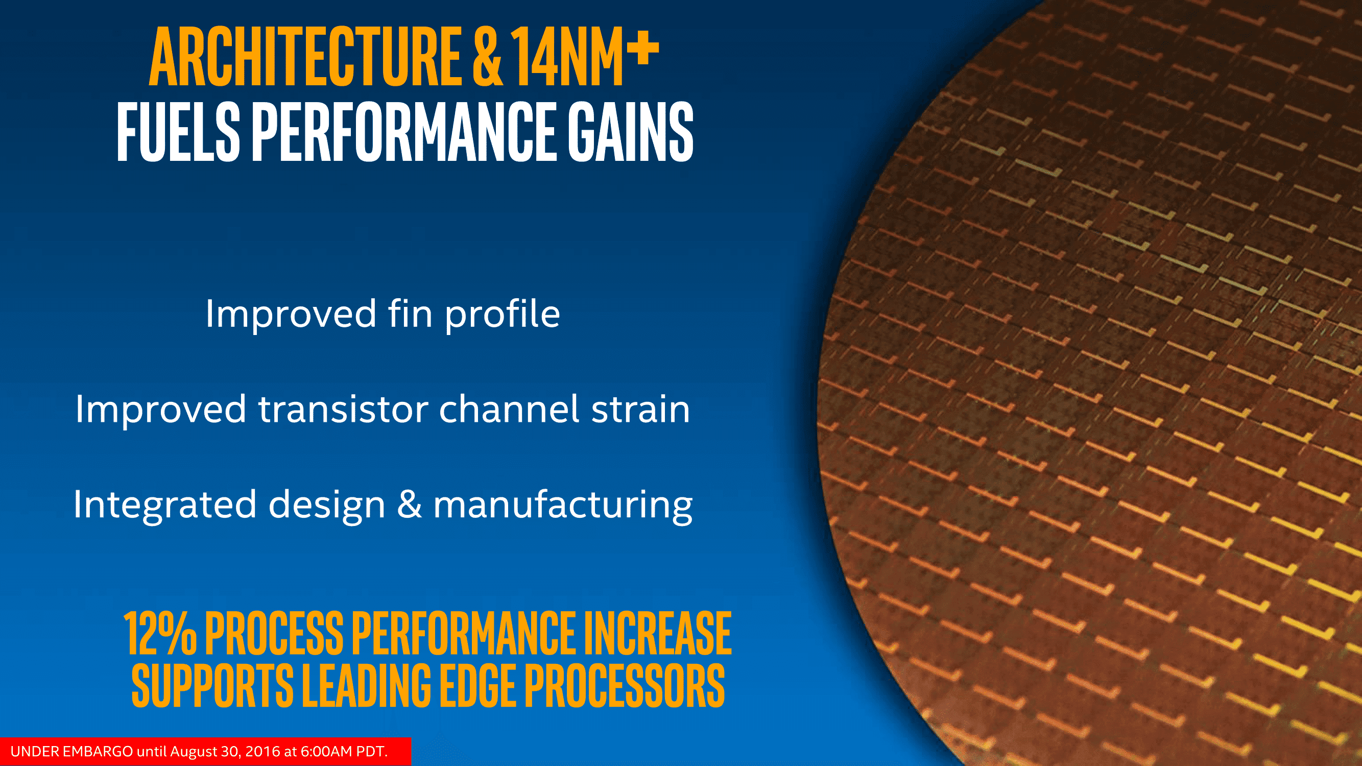
This means three bites of the cherry for 14nm before we see 10nm in prime time. First it was Broadwell, then Skylake, and today Intel is announcing Kaby Lake. As part of the release, Intel has mentioned that a number of key benefits for Kaby Lake will be based on an optimized 14nm process, called 14PLUS (or 14nm+, 14FF+). This process as a quick summary has a higher fin height and larger pitch, essentially giving a less-dense set of transistors that have more room to breathe. Normally a larger pitch means more voltage required, but this is offset by the fin height and Intel says is good for another few hundred MHz for performance. The less-dense design, in theory, may also help in overclocking, however we will have to wait until January to see those results.
Today’s Announcement
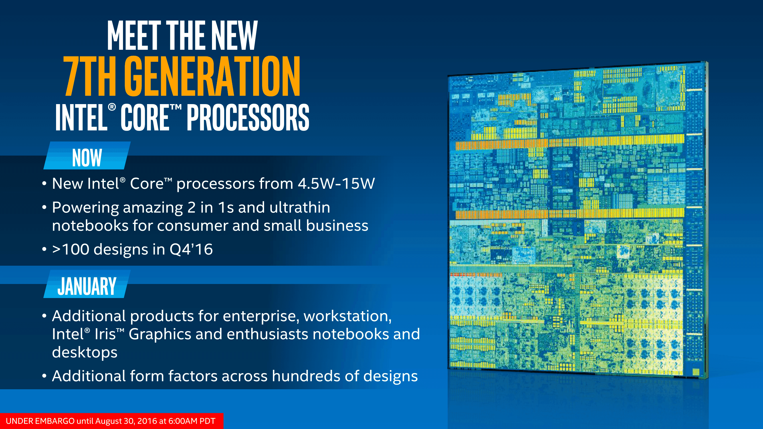
The reveal today covers several aspects of Kaby Lake. First is the actual SKUs that will be launched, which consist of three Kaby Lake-Y parts around 4.5W aimed at high-end tablets and 2-in-1 devices and three Kaby Lake-U parts at 15W for notebooks. Both sets of KBL-Y and KBL-U CPUs will feature in mini-PCs as well, so we expect to see the usual array of Zotac and ECS announcements in due course. We have details on all six CPUs to give you, including the new Core M branding regime for the 4.5W family of parts.
The pre-briefings we have had go into some detail regarding changes in the processor, particularly regarding the new enhanced media blocks inside the GPU to support new encode/decode features. The graphics power, in terms of EUs or the microarchitecture, hasn’t changed but the fixed function hardware has some nice upgrades for an updated version of Gen 9 graphics aimed at the upcoming era of 4K support. Ganesh has gone into detail for us over what that means, especially where power and battery life is concerned for anyone creating/consuming 4K content.
Kaby Lake also has an updated Speed Shift package, to accelerate the work already done with Skylake in boosting the performance of the CPU quicker to save power. Intel call it a refinement in the mechanism of handing frequency control back from the OS to the CPU, however ‘Speed Shift v2’ is an adequate moniker to show the upgraded difference.
Intel hasn’t gone into much detail regarding the new 14nm+ process itself in terms of specifics, but has listed a number of performance gains that come out of the new CPU. The fundamental microarchitecture between Skylake and the new Kaby Lake parts is practically unchanged (DMI 3.0 now allows PCIe 3.0 x4 NVMe drives from the integrated PCH), but the updated fin profile and reduced ‘strain’ by the larger fin pitch is being quoted as giving a 12% performance increase due to process alone, typically through additional frequency for the same power. The main benefits to KBL will be in that frequency due to the 14nm+ process as well as the new media capabilities.
As always, Intel consistently emphasizes the difference between a new notebook/2-in-1 based on a 15W Kaby Lake processor compared to a 5-year old device, such one based on a mobile Sandy Bridge ULV part. Intel continually sees its market revolving around new experiences created by new form factors, and to generate revenue requires people to upgrade and decide how these new experiences can influence an upgrade. Intel expects to have over 100 Kaby Lake system designs in the consumer channel by Q4, including 120+ using Thunderbolt 3, 100+ using Windows Hello (either via a Real Sense camera or a fingerprint sensor), 50+ designs with 4K UHD as a primary feature and 25+ designs with contact enabled pens. Kaby Lake should be pin compatible with Skylake based designs, meaning that for a number of cases we will simply see a drop in, but others will have new design IDs on show.
One of the first things that users may notice about the new Kaby Lake processors is that the KBL-Y series is dropping both the m5 and my naming scheme from its segment. We will see m3 still, but this will now be paired with i5 and i7. Intel isn’t specifying that m5 or m7 have gone away entirely, but it doesn’t seem to be a part of the KBL-Y arrangement this time around.
There are a couple of reasons for this – the one Intel discussed with us is that it comes down to performance and OEM requests. An i5 in a 4.5W form factor (or as high as 7W in cTDP Up) performs essentially on par with the KBL-U i5 parts, and OEM customers requested that the naming scheme change to reflect that. The sense of parity and brand between the two, especially when customers look at a device for less than a couple of minutes and anything that they feel familiar with tends to be a bonus.
The other reason is perhaps that the Core M brand as a whole hasn’t taken off as Intel thought it would, or ‘m’ is associated with low power, low performance, or essentially ‘mobile’. So one could argue that renaming m5 to i5 is purely a mental adjustment tactic, however I’d hazard a guess and say that if they were called i5 and i7 to begin with, no-one would have batted an eye-lid at the difference. Interestingly enough, it is the i7 version of Kaby Lake-Y that has the highest single core turbo frequency mode out of all the processors being launched today, even the 15W parts. 3.6 GHz for a 4.5W TDP processor is nothing to be sniffed at, although it will depend on the device and OEM configuration that will determine just how long it stays at 3.6 GHz.
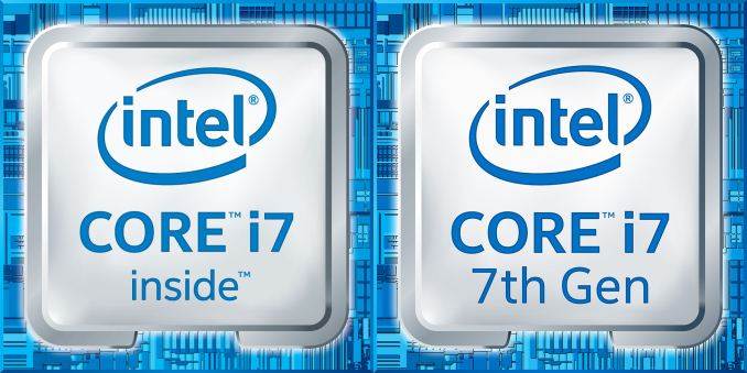
Finally, along with the change in how 4.5W parts are branded, Intel has also changed how this information is presented to consumers. The Intel case badge and similar marketing/identification material now includes the processor generation along with its designation. So instead of simply being a “Core i7” of unknown generation, Kaby Lake devices will be badged “Core i7, 7th Gen.” This should make it a bit clearer which devices are Kaby Lake versus Skylake, though it does raise the question over whether this will hurt Intel at all once Cannonlake (8th Gen) ships.
Skylake vs. Kaby Lake Branding
The Starting Lineup: 2+2
Like Broadwell in 2014, the 2016 launch of Kaby Lake is a bottom-up launch. This means that Intel is starting with the small die, low power Y & U series processors, and then will move further up the stack later on. So all 6 SKUs launching today – 3 at 4.5W and 3 at 15W – are based on the same 2+2 die. This means 2 CPU cores paired with a GT2 iGPU.
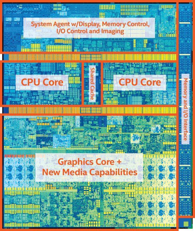
Intel has not disclosed the die size of their 2+2 Kaby Lake die at this time. This likely has something to do with the underlying 14nm+ process being used for Kaby Lake, which has left Intel a bit mum to start with (more on this later). At any rate, the Kaby Lake 2+2 die is not remarkably different in layout or design from Skylake. The big changes are under the hood: the 14nm process, and the GPU media processor improvements introduced with Kaby Lake.
The New Processors
Without further ado, here are the processors. First up, the KBL-Y 4.5W Parts, along with an m7 from Skylake for comparison:
| Intel 7th Gen (Kaby Lake) Y-Series Lineup | ||||
| i7-7Y75 | i5-7Y54 | m3-7Y30 | m7-6Y75 (Skylake) |
|
| Cores | 2 | 2 | 2 | 2 |
| Threads | 4 | 4 | 4 | 4 |
| Base CPU Freq. | 1.3 GHz | 1.2 GHz | 1.0 GHz | 1.2 GHz |
| Turbo CPU Freq. | 3.6 GHz | 3.2 GHz | 2.6 GHz | 3.1 GHz |
| Graphics | HD 615 (GT2) | HD 615 (GT2) | HD 615 (GT2) | HD 515 (GT2) |
| EUs | 24 | 24 | 24 | 24 |
| iGPU Freq. | ? | ? | ? | 1 GHz |
| TDP | 4.5W | 4.5W | 4.5W | 4.5W |
| DDR3L Freq. | 1600MHz | 1600MHz | 1600MHz | 1600MHz |
| LPDDR3… | ||||


