
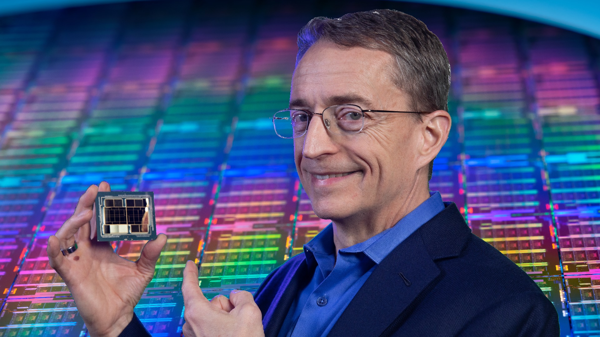
Earlier this 12 months, new Intel CEO Pat Gelsinger outlined his new ‘IDM 2.0’ imaginative and prescient for Intel. This imaginative and prescient was a three-pronged technique based mostly on bettering its personal course of node expertise, mixing in different foundry expertise the place wanted, and likewise realigning its manufacturing for a brand new foundry service providing permitting different semiconductor corporations to make use of Intel’s manufacturing experience. As a part of the journey in the direction of Gelsinger’s IDM 2.Zero imaginative and prescient, we have been instructed to count on updates at a extra common cadence, and the announcement of ‘Intel Accelerated’ in a few weeks is the following occasion on the calendar.
Intel IDM 2.0
As AnandTech reported again in March, Intel’s IDM 2.Zero technique options the next:
- Build (on Intel 7nm)
- Expand (use TSMC and others)
- Productize (Intel Foundry Services)
Previously Intel was nearly fully insular, preferring to make use of its personal applied sciences nearly solely, and it stored them to itself. Through IDM 2.0, CEO Pat Gelsinger is hoping to drive Intel’s subsequent wave of merchandise through the use of the perfect the market has to supply, but in addition broaden Intel’s personal manufacturing to new clients as a possible income stream. The guise of this improvement can be within the sense of aligning semiconductor manufacturing exterior of Asia, to make different areas of the world much less reliant on a single useful resource.
Part of this technique requires Intel to execute on its analysis roadmaps. Intel’s struggles to allow 10nm in suitably excessive volumes have been the main focus of loads of column inches, and whereas Intel is now transport 10nm Tiger Lake-H within the tens of millions* and 10nm Ice Lake Xeons within the tons of of 1000’s*, there’s a want to handle the way forward for Intel’s manufacturing. This means ensuring it aligns with industrial pursuits and allows a aggressive providing in opposition to the competitors. This covers not solely manufacturing, to which Intel introduced a $20b funding in its Arizona manufacturing earlier this 12 months, but in addition superior packaging applied sciences, the place Intel introduced a $3.5b funding in its New Mexico services in May.
Intel’s Ocotillo Campus, Arizona
Part of making its Intel Foundry Services providing for exterior events to make use of Intel manufacturing depends on Intel being extra open about its expertise and showcasing progress in its analysis and improvement, maybe to a level greater than it has achieved prior to now. Any future clients of Intel’s IP portfolio will need to know what’s coming down the pipe, particularly when silicon improvement takes years and getting the fitting timing within the alignment of applied sciences turns into essential in these aggressive markets. Having a platform to showcase Intel’s roadmaps is what this upcoming Intel Accelerated Webcast appears to be about.
Intel Accelerated
On Monday July 26th, 2pm Pacific, Intel will livestream its Intel Accelerated webcast. The subjects of the day are shows from CEO Pat Gelsinger and Dr. Ann Kelleher on Intel’s course of node expertise improvement and roadmaps into Intel’s packaging portfolio. Dr. Ann Kelleher is Intel’s SVP and GM of Technology Development, and the particular person in control of all of this.
We are hoping that this webcast will go into element as to the place Intel expects its 10nm improvement to go on SuperFin/Enhanced SuperFin, main into discussions about 7nm. While Intel gained’t be discussing issues like buried energy rails or new manufacturing strategies, we are going to hopefully see a disclosure extra akin to TSMC and Samsung’s Foundry occasions that occur yearly concerning what variations of course of node improvement are being focused.
On the packaging entrance, we all know that Intel has EMIB, Foveros, and ODI underneath analysis up in opposition to TSMC’s 3DFabric, so insights into how Intel is creating its expertise will probably be…


