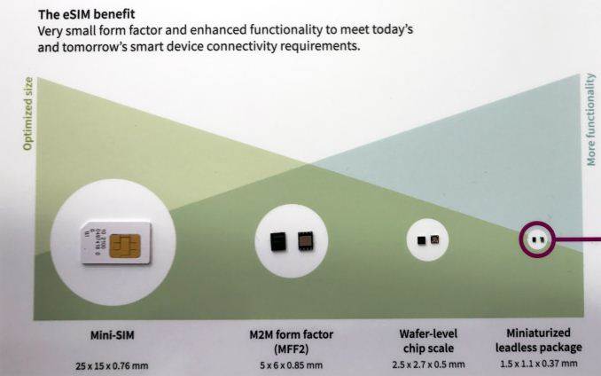
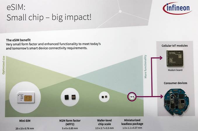
At MWC this year, Infineon showcased a lineup of its current and embedded SIM products. The company demonstrates not only the industry-standard MFF2 eSIM chip, but also considerably smaller ICs designed for future miniature devices (many of which may not even exist yet as a category) as well as M2M (machine to machine) applications. It is noteworthy that to manufacture an eSIM the size of a match head, Infineon uses GlobalFoundries 14LPP process technology, taking advantage of leading-edge lithography to bring the size of a simple device down.
The first SIM cards were introduced in 1991 along with the world’s first GSM network operated by Radiolinja in Finland (now the company is called Elisa). Back then, mobile phones were so bulky that a card the size of a credit card (1FF) could fit in. Eventually, handsets got smaller, Mini-SIMs (2FF) replaced full-sized SIMs and then Micro-SIM (3FF) and Nano-SIM (4FF) cards took over. While mobile phones have evolved considerably in terms of feature-set in the last 25 years, the function of the SIM card remained the same: it stores an integrated circuit card identifier (ICCID), an international mobile subscriber identity (IMSI), a location area identity, an authentication key (Ki, this part actually requires a basic 16- or 32-bit compute unit) as well as a phone book and some SMS messages.
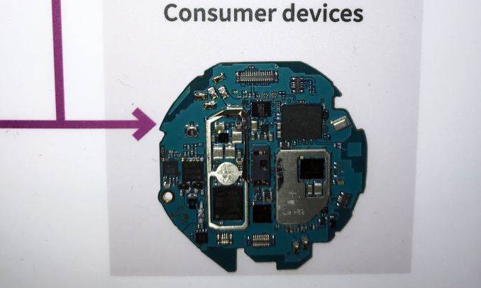
By today’s standards, the amount of data that each SIM card stores is so tiny that its physical dimensions are simply not justified. Even Nano-SIMs are too large for applications like a smartwatch, and this is when embedded SIMs come into play: their form-factor is considerably smaller, they can be used with various operators (which makes them more flexible in general) and some of such cards have an expanded feature set (e.g., hardware crypto-processors). Today, there is one internationally recognized form-factor for eSIMs, the MFF2, which is used inside devices like Samsung’s Gear series smartwatch with GSM/3G connectivity. If we actually take a look inside the Gear S2 smartwatch, we will notice that the eSIM is actually one of the largest components and its functionality is disproportional to its dimensions.

At MWC 2017 Infineon is demonstrating two more eSIM implementations, which have not been standardized (yet?), but which are already used inside millions of devices.

The first one, when packaged, has dimensions of 2.5×2.7×0.5 mm, which essentially means that it has no packaging at all. This IC is produced using a mature 65 nm process technology and that means that it is very cheap.
The second eSIM implementation that Infineon demonstrates is actually even tinier: its dimensions when fully packaged and ready to use are just 1.5×1.1×0.37 mm. The IC is made using 14LPP process technology by GlobalFoundries and the foundry charges the chip developer accordingly. Using a leading-edge process technology to make eSIM cards is not something common, but the approach enables developers of various devices to take advantage of the smallest cards possible (another advantage of such cards are low voltages and power consumption).

It remains to be seen when the industry formally adopts eSIM standards smaller than the MFF2, but dimensions of the eSIMs that Infineon is demonstrating clearly indicate that there are ways to make these cards smaller. Moreover, companies are not afraid of using proprietary/non-standard form-factors are already using the offerings from Infineon. It is up for debate whether using leading-edge process technology for making eSIMs makes sense in general (after all, far not all devices require tiny dimensions and expanded functionality of eSIMs, such as crypto-processors), but with 10 million non-standard eSIMs shipped to date it is obvious that there are mass market devices that can absorb such chips even at potentially premium pricing.


