
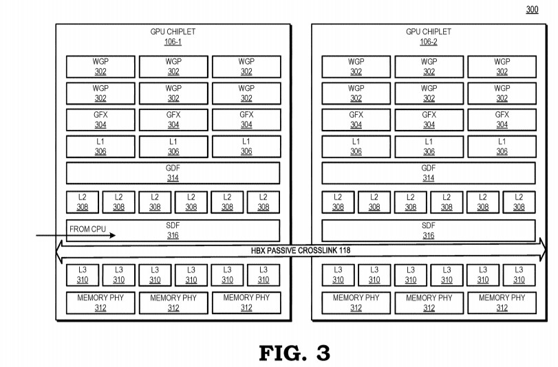
AMD studies that the usage of a number of GPU configuration is inefficient attributable to restricted software program help, so that’s the reason why GPUs have been saved monolithic for years. However, it looks like the corporate has discovered a technique to go previous the constraints and implement a adequate resolution. AMD believes that by utilizing its new excessive bandwidth passive crosslinks, it may possibly obtain splendid chiplet-to-chiplet communication, the place every GPU within the chiplet array can be coupled to the primary GPU within the array. All the communication would undergo an energetic interposer which might comprise many layers of wires which might be excessive bandwidth passive crosslinks. The firm envisions that the primary GPU within the array would communicably be coupled to the CPU, which means that it should use the CPU probably as a communication bridge for the GPU arrays. Such a factor would have massive latency hit so it’s questionable what it means actually.
The patent additionally suggests that every GPU chiplet makes use of its personal Last Level Cache (LLC), as a substitute of separate LLCs for every GPU, so every of the LLCs is communicably coupled and the cache stays coherent throughout all chiplets. Rumors recommend that we’re going to see the primary chiplet-based structure from AMD as successor to the RDNA3 era, so it would occur within the coming years. AMD already has expertise with chiplets from its processors, with Ryzen processors being the prime instance. We simply want to attend and see the way it will look as soon as it arrives for GPUs.


