
The AMD crew shocked us right here. What appeared like a really par-for-the-course Computex keynote become an unimaginable demonstration of what AMD is testing within the lab with TSMC’s new 3D Fabric applied sciences. We’ve lined 3D Fabric earlier than, however AMD is placing it to good use by stacking up its processors with extra cache, enabling super-fast bandwidth, and higher gaming efficiency. That’s the declare at any fee, and AMD showcased its new demo processor on stage at Computex. Here’s a deeper run-down into what it truly is.
3D Chiplets: The Next Step
AMD introduced it was wanting into 3D stacking applied sciences with ‘X3D’ again in March 2020 at its Financial Analyst Day, with a really odd diagram exhibiting a chiplet processor with what seemed like stacks of HBM or some type of reminiscence across the outdoors. At the time AMD stated it was a mixture of 2.5D and 3D packaging applied sciences enabling 10x bandwidth density or greater. The ‘X’ in ‘X3D’ was meant to face for Hybrid, and the know-how was set for ‘the future’. Since then TSMC has introduced its 3D Fabric line of applied sciences, a broad identify for its mixture of two.5D and 3D integration choices.
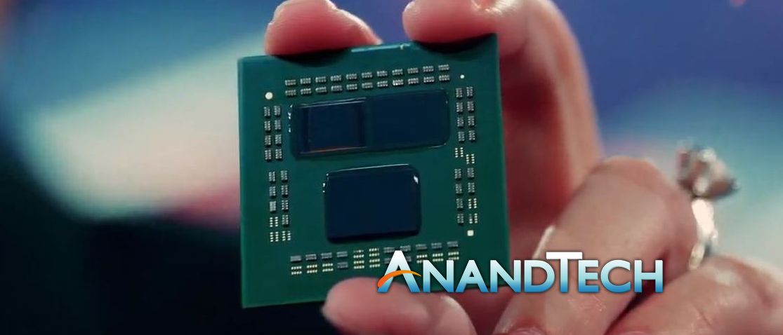
Today AMD offered the primary stage of its 3D chiplet journey. The first utility is a stacked cache on high of a normal processor chiplet. On stage, Lisa Su showcased one in every of AMD’s Ryzen 5000 dual-chiplet processors with Zen three cores. On one of many compute chiplets, a 64 MB SRAM constructed on TSMC’s 7nm was built-in on the highest, successfully tripling the quantity of cache that the cores have entry to.
That implies that the unique Ryzen 5000 chiplet, with eight cores getting access to 32 MB of L3 cache, now turns into an eight-core complicated with entry to 96 MB of L3 cache. The two dies are bonded with Through Silicon Vias (TSVs), passing energy and information between the 2. AMD claims that the entire bandwidth of the L3 cache will increase to past 2 TB/sec, which might technically be sooner than the L1 cache on the die (however with greater latency).
As a part of the chip diagram, the TSVs could be direct copper-to-copper bonding. The cache die isn’t the identical dimension because the core complicated, and because of this extra structural silicon is required to make sure that there’s equal strain throughout each the underside compute die and the highest cache die. Both dies are thinned, with the aim to allow the brand new chiplet in the identical substrate and heatspreader know-how at present in use in Ryzen 5000 processors.
The prototype processor proven on stage had one in every of its chiplets utilizing this new caching know-how. The different chiplet was left as normal to indicate the distinction, and the one chiplet that had the cache die ‘exposed’ made it apparent and comparable with the common non- built-in chiplet. CEO Dr. Lisa Su stated that the 64 MB SRAM on this case is a 6mm x 6mm design (36 mm2), which places it at slightly below half the die space of a full Zen three chiplet.
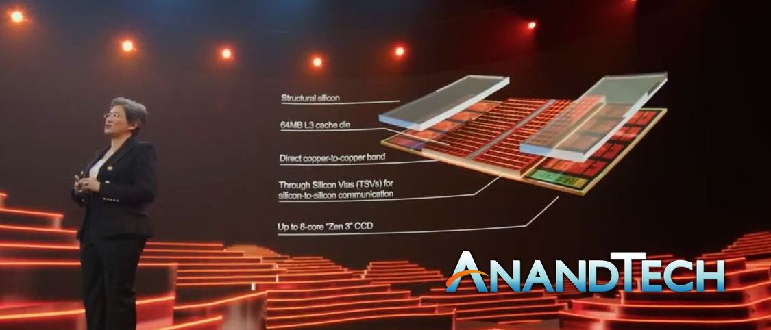
In a full product Lisa defined that each one the chiplets would have the stacked cache enabled, for 96 MB of cache per chiplet, or 192 MB whole for a processor like this that has 12 or 16 cores.
As a part of the know-how, it was defined that this packaging permits a >200x interconnect density in comparison with common 2D packaging (which is one thing we already know from HBM stacking), a >15x density improve in comparison with microbump know-how (a shot straight throughout the bow of Intel’s Foveros), and >3x higher interconnect effectivity in comparison with microbumps. The TSV interface is a direct die-to-die copper interconnect, which means that AMD is utilizing TSMC’s Chip-on-Wafer know-how. Dr Su claimed on stage that these options make this essentially the most superior and versatile ‘active-on-active’ chip stacking know-how within the trade.
As for efficiency…


