
Intel’s first foray into 14nm was with its Broadwell product portfolio. It launched into the cell market with a wide range of merchandise, nonetheless the desktop providing in 2015 was extraordinarily restricted – solely two socketed desktop processors ever made it to retail, and in restricted portions. This is regardless of customers ready for a robust 14nm replace to Haswell, but in addition due to the best way Intel constructed the chip. Alongside the processor was 128 MB of eDRAM, a kind of extra cache between the CPU and the principle reminiscence. It brought on fairly a stir, and we’re retesting the {hardware} in 2020 to see if the idea of eDRAM remains to be definitely worth the effort.
eDRAM: The Savior
In latest years, Intel has pushed laborious its notorious ‘Pyramid of Optane’, designed to showcase the tradeoff between small quantities of cache reminiscence near the CPU being low latency, out to the massive offline storage supplied for at a big ping time. When a processor requires information and directions, it navigates this hierarchy, with the objective to have as a lot of what’s required as near the CPU (and due to this fact as quick) as potential.
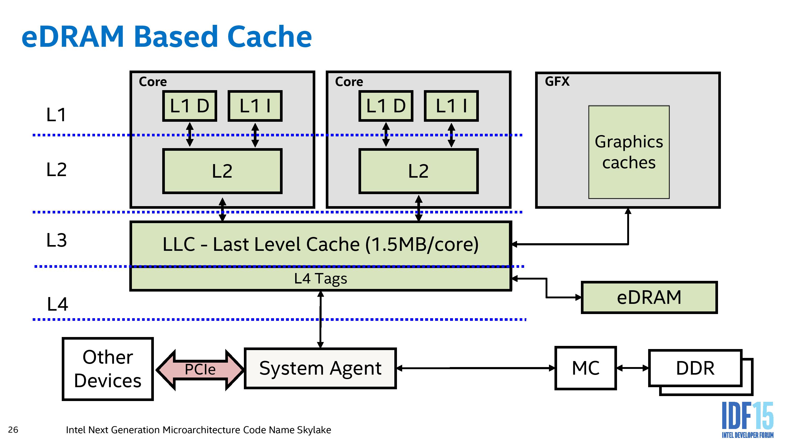
Traditional trendy x86 processors comprise three ranges of caches, every rising in measurement and latency, earlier than reaching most important reminiscence, after which out to storage. What eDRAM does is add a fourth layer between the final L3 cache on the processor. Whereas the L3 is measured in single digit megabytes, the eDRAM is within the 10s-100s of megabytes, and DRAM measures in gigabytes. Whereas the L3 cache is positioned on the processor die and low latency, the eDRAM is barely greater latency, and the principle reminiscence is on modules outdoors the processor socket on the highest latency. Intel enabled an ‘eDRAM’ layer as a separate piece of silicon with the processor package deal, as much as 128 MiB, providing latency and bandwidth between the L3 and most important reminiscence.
This piece of silicon was constructed on Intel’s 22nm IO manufacturing course of, slightly than 22nm SoC or 14nm, attributable to Intel’s capability to drive greater 22nm frequencies on the time.
By maintaining the eDRAM as a separate piece of silicon, it allowed Intel to regulate inventory ranges based mostly on demand – if the product failed, there would nonetheless be loads of smaller CPU die for packaging. Even at this time, processors made with additional eDRAM use the identical die as seen again in 2013-2015, exhibiting the longevity of the product. The first eDRAM merchandise had been cell beneath the 22nm Haswell microarchitecture, however Broadwell noticed it come to desktop.
On the Broadwell processors, this resulted in a reminiscence entry layer with the next efficiency:
| Broadwell Cache Structure | ||||
| AnandTech | Size | Type | Latency | Bandwidth |
| L1 Cache | 32 KiB / core | Private | 4-cycle | 880 GiB/s |
| L2 Cache | 256 KiB / core | Private | 12-cycle | 350 GiB/s |
| L3 Cache | 6 MiB | Shared | 26-50 cycle | 175 GiB/s |
| eDRAM | 128 MiB | Shared | < 150 cycle | 50 GiB/s |
| DDR3-1600 | Up to 16 GiB | Shared | 200+ cycle | 25.6 GiB/s |
The simplistic view of this eDRAM was as a ‘level 4’ cache layer – that is in the end the way it was described to us on the time, with the eDRAM layer performing as a sufferer cache accepting L3 evictions however enabled via a shadow tag system accessed via the L3. Data wanted from the eDRAM must be moved again into L3 earlier than going wherever else, together with the graphics or the opposite IO or most important reminiscence. In order to do that, these shadow tags required roughly 0.5 MiB/core of the L3 cache, lowering the L3 usefulness in change for decrease latency extending out to 128 MiB. This is why Broadwell solely had 1.5 MiB/core of L3 cache, slightly than the total 2.Zero MiB/core that the die shot recommended it ought to have.
Haswell/Broadwell eDRAM Layout
The eDRAM might be dynamically break up on the fly for CPU or GPU requests,…


 assessment: a strong")


